NTE7040 データシートの表示(PDF) - NTE Electronics
部品番号
コンポーネント説明
メーカー
NTE7040 Datasheet PDF : 3 Pages
| |||
Electrical Characteristics: (TA = +25°C, ±B1 = ±25V, +B2 = 25V, RL = 8Ω, Rg = 600Ω unless
otherwise specified)
Parameter
Symbol
Test Conditions
Min Typ Max Unit
Quiescent Current
Output Offset Voltage
Input Resistance
Voltage Gain (Closed Loop)
Voltage Gain (Open Loop)
Output Power
Total Harmonic Distortion
Output Noise Voltage
Supply Voltage Rejection Ratio
+IQ1 Vin = 0
between +B1 and Pin5 20
+IQ2
between +B2 and Pin6 –
–IQ1
between –B1 and Pin12 –
∆VO Vin = 0, between Pin3 and GND
–
Rin f = 1kHz, R102 = 56kΩ
–
GV f = 1kHz, R103 = 680Ω, R104 = 56kΩ –
GV(OL) f = 1kHz, R103 = 0
–
PO1 f = 20kHz, THD = 0.5%, RL = 8Ω 15
PO2 Note 2
THD = 0.7%, RL = 4Ω 15
THD f = 20kHz, Pout = 2W
–
Vn Rg = 5.1kΩ, BW = 20Hz to 20kHz
–
SVR Rg = 5.1kΩ, fripple = 100Hz (at Pin12) 52
60 120 mA
– 22 mA
– 152 mA
0 ±0.1 V
55 – kΩ
38 – dB
88 – dB
18 – W
18 – W
0.04 0.20 %
0.35 0.50 mV
60 – dB
Note 2. Standard test conditions are as follows: PO1: ±B1 = ±22V, PO2: ±B1 = ±19V
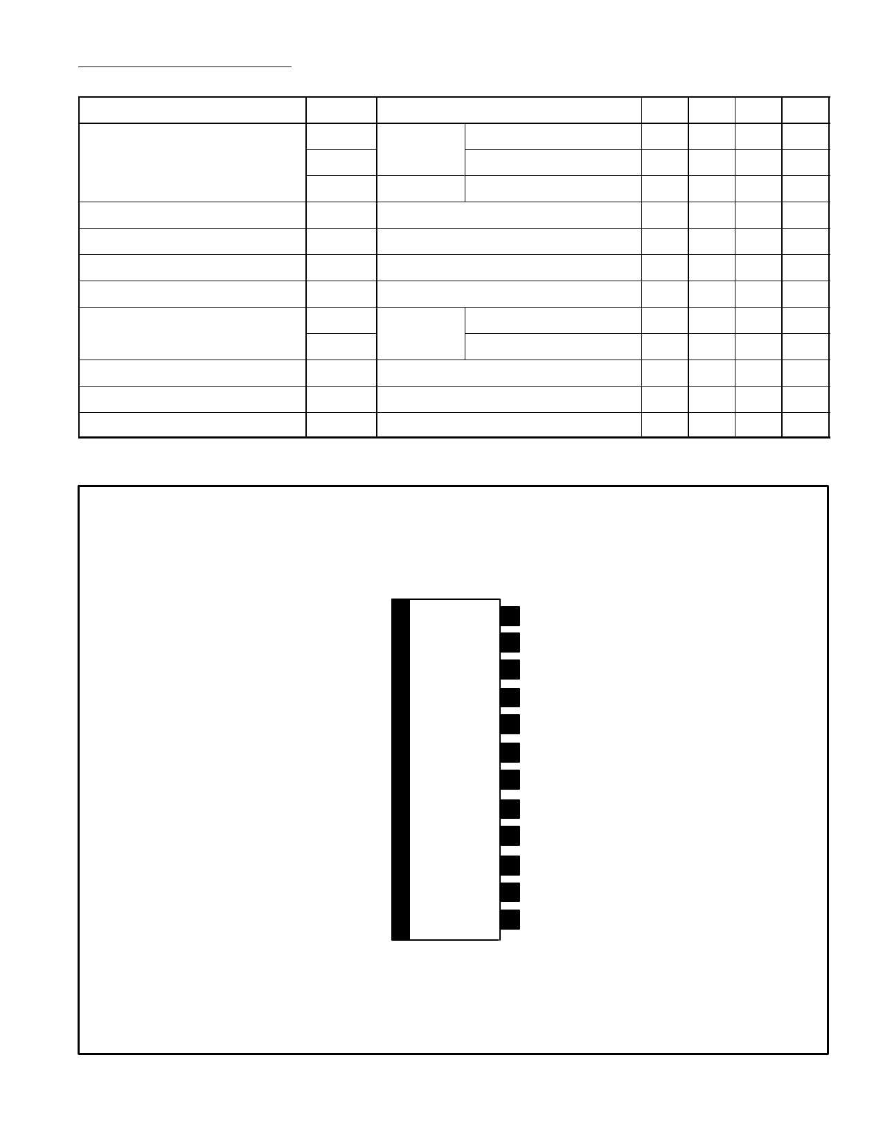
Pin Connection Diagram
(Front View)
12 GND
11 Ripple Rejection
10 Input
9 Input
8 Compensation
G
7 Compensation
N
D
6 Muting Input
5 VCC
4 N.C.
3 Output
2 N.C.
1 N.C.
Share Link: 