NTE2055 データシートの表示(PDF) - NTE Electronics
部品番号
コンポーネント説明
メーカー
NTE2055 Datasheet PDF : 4 Pages
| |||
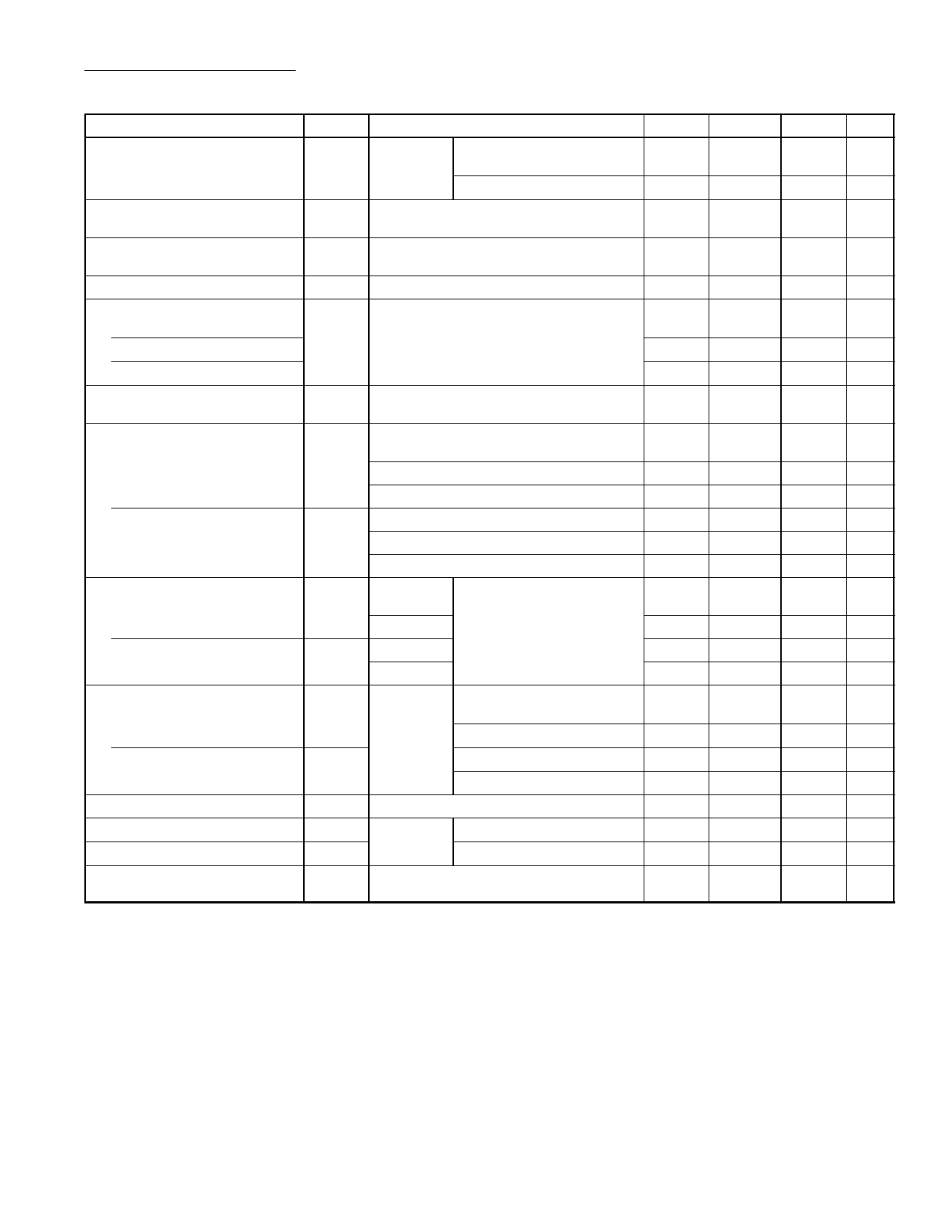
Electrical Characteristics: (CI = 0.1µF mylar, RI = 470kΩ @ Vref = 2V, RI = 27kΩ @ Vref = 200mV,
RC = 300kΩ, TA = +25°C ; all voltages referenced to Analog GND, Pin1, unless
otherwise specified)
Parameter
Symbol
Test Conditions
Min
Typ
Max Unit
Linearity–Output Reading
Stability – Output Reading
Symmetry – Output Reading
VDD = 5V,
VEE = –5V,
Note 2
Vref = 2.000V
Vref = 200.0mV
VDD = 5V, VEE = –5V, VX = 199mV,
Vref = 200mV
VDD = 5V, VEE = –5V, Vref = 2000mV,
Note 3
–0.05
– Count
–
–
±0.05
±0.05
–
+0.05 %rdg
+ Count
– %rdg
3
LSD
–
–
4
LSD
Zero–Output Reading
Bias Current
Analog Input
Reference Input
VDD = 5V, VEE = –5V, VX = 0V, Vref = 2V
–
VDD = 5V, VEE = –5V
–
–
0
0
LSD
±20
±100
pA
±20
±100 pA
Analog GND
–
±20
±500 pA
Common Mode Rejection
Input Voltage (Pin9, Pin10)
“0” Level
“1” Level
Output Voltage (Pin14 to Pin23)
“0” Level
“1” Level
Output Current (Pin14 to Pin23)
Source
Sink
Input Current (DU, Pin9)
Quiescent Current
DC Supply Rejection
VDD = 5V, VEE = –5V, fClk = 32kHz,
VX = 1.4V, Vref = 2V
–
65
–
dB
VIL
VDD = 5V, VO = 4.5V or 0.5V, Note 3
VDD = 10V, VO = 9V or 1V, Note 3
VDD = 15V, VO = 13.5V or 1.5V, Note 3
VIH VDD = 5V, VO = 0.5V or 4.5V, Note 3
VDD = 10V, VO = 1V or 9V, Note 3
VDD = 15V, VO = 1.5V or 13.5V, Note 3
–
2.25
–
4.50
–
6.75
3.5
2.75
7.0
5.50
11.0
8.25
1.5
V
3.0
V
4.0
V
–
V
–
V
–
V
VOL
VOH
VSS = 0V
VSS = –5V
VSS = 0V
VSS = –5V
VDD = 5V, VEE = –5V
–
–
4.95
4.95
0
–5.0
–5.0
5.0
0.05
V
–4.95 V
–
V
–
V
IOH
VDD = 5V,
VSS = 0V, VOH = 4.6V
VEE = –5V VSS = –5V, VOH = 4.5V
–0.2
–0.5
–0.36
–0.9
–
mA
–
mA
IOL
VSS = 0V, VOL = 0.4V
0.51
0.88
–
mA
VSS = –5V, VOL = –4.5V
1.3
2.25
–
mA
IDU VDD = 5V, VEE = –5V
–
±0.00001 ±0.3
µA
IQ
VDD to VEE, VDD = 5V, VEE = –5V
ISS = 0
VDD = 8V, VEE = –8V
–
0.9
2.0
mA
–
1.8
4.0
mA
VDD = 5V, VEE = –5V, VDD to VEE, ISS = 0,
–
0.5
– mV/V
Vref = 2V
Note
Note
Note
2. Accuracy – The accuracy of the meter at full scale is the accuracy of the setting of the reference volt-
age. Zero is recalculated during each conversion cycle. The meaningful specification is linearity.
In other words, the deviation from correct reading for all inputs other than positive full scale and zero
is defined as the linearity specification.
3. Symmetry – Defined as the difference between a negative and positive reading of the same voltage
at or near full scale.
4. Referenced to VSS for Pin9. Referenced to VEE for Pin10.
Share Link: 