24AA02 データシートの表示(PDF) - Microchip Technology
部品番号
コンポーネント説明
メーカー
24AA02 Datasheet PDF : 24 Pages
| |||
24AA02/24LC02B
2K I2C™ Serial EEPROM
Device Selection Table
Part
Number
VCC
Range
Max Clock
Frequency
24AA02
1.8-5.5
400 kHz(1)
24LC02B 2.5-5.5
400 kHz
Note 1: 100 kHz for VCC <2.5V
Temp
Ranges
I
I, E
Features
• Single supply with operation down to 1.8V
• Low-power CMOS technology
- 1 mA active current typical
- 1 µA standby current typical (I-temp)
• Organized as 1 block of 256 bytes (1 x 256 x 8)
• 2-wire serial interface bus, I2C™ compatible
• Schmitt Trigger inputs for noise suppression
• Output slope control to eliminate ground bounce
• 100 kHz (24AA02) and 400 kHz (24LC02B)
compatibility
• Self-timed write cycle (including auto-erase)
• Page write buffer for up to 8 bytes
• 2 ms typical write cycle time for page write
• Hardware write-protect for entire memory
• Can be operated as a serial ROM
• Factory programming (QTP) available
• ESD protection > 4,000V
• 1,000,000 erase/write cycles
• Data retention > 200 years
• 8-lead PDIP, SOIC, TSSOP and MSOP packages
• 5-lead SOT-23 package
• Pb-free finish available
• Available for extended temperature ranges:
- Industrial (I): -40°C to +85°C
- Automotive (E): -40°C to +125°C
Description
The Microchip Technology Inc. 24AA02/24LC02B
(24XX02*) is a 2 Kbit Electrically Erasable PROM. The
device is organized as one block of 256 x 8-bit memory
with a 2-wire serial interface. Low-voltage design
permits operation down to 1.8V, with standby and
active currents of only 1 µA and 1 mA, respectively.
The 24XX02 also has a page write capability for up to
8 bytes of data. The 24XX02 is available in the
standard 8-pin PDIP, surface mount SOIC, TSSOP and
MSOP packages and is also available in the 5-lead
SOT-23 package.
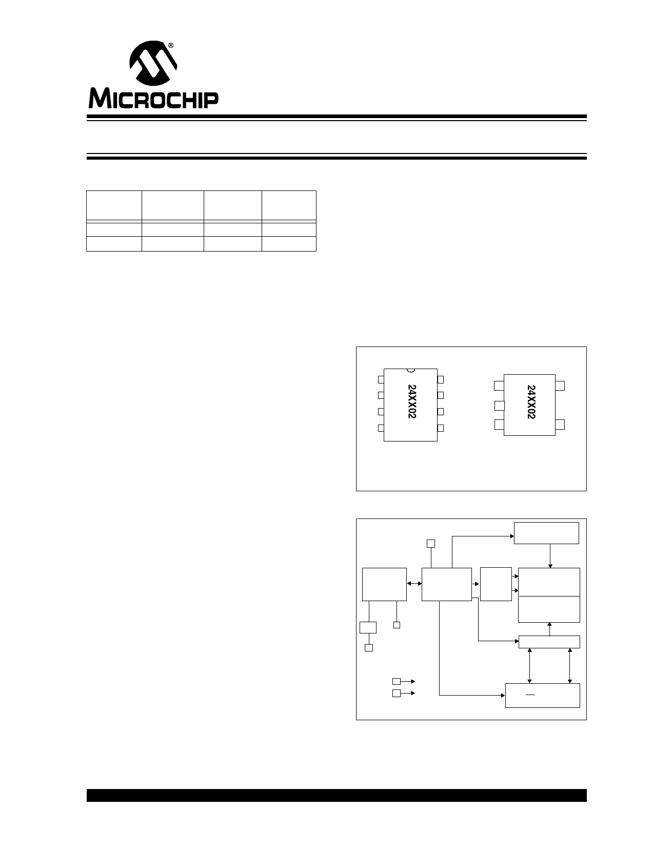
Package Types
PDIP/SOIC/TSSOP/MSOP SOT-23-5
A0 1
A1 2
A2 3
Vss 4
8 Vcc SCL 1
7 WP
6 SCL Vss 2
5 SDA SDA 3
5 WP
4 Vcc
Note: Pins A0, A1 and A2 are not used by the
24XX02. (No internal connections).
Block Diagram
WP
HV
Generator
I/O
Control
Logic
I/O
SCL
SDA
VCC
VSS
Memory
Control XDEC
Logic
EEPROM
Array
Page
Latches
YDEC
Sense Amp.
R/W Control
2003 Microchip Technology Inc.
DS21709C-page 1
Share Link: 