MT8888C データシートの表示(PDF) - Mitel Networks
部品番号
コンポーネント説明
メーカー
MT8888C Datasheet PDF : 16 Pages
| |||
MT8888C/MT8888C-1
®
Integrated DTMF Transceiver
with Intel Micro Interface
Features
• Central office quality DTMF transmitter/receiver
• Low power consumption
• High speed Intel micro interface
• Adjustable guard time
• Automatic tone burst mode
• Call progress tone detection to -30dBm
Applications
• Credit card systems
• Paging systems
• Repeater systems/mobile radio
• Interconnect dialers
• Personal computers
Description
The MT8888C is a monolithic DTMF transceiver with
call progress filter. It is fabricated in CMOS
technology offering low power consumption and high
reliability.
ISSUE 2
May 1995
Ordering Information
MT8888CE/CE-1 20 Pin Plastic DIP
MT8888CC/CC-1 20 Pin Ceramic DIP
MT8888CS/CS-1 20 Pin SOIC
MT8888CN/CN-1 24 Pin SSOP
-40°C to +85°C
The receiver section is based upon the industry
standard MT8870 DTMF receiver while the
transmitter utilizes a switched capacitor D/A
converter for low distortion, high accuracy DTMF
signalling. Internal counters provide a burst mode
such that tone bursts can be transmitted with precise
timing. A call progress filter can be selected allowing
a microprocessor to analyze call progress tones.
The MT8888C utilizes an Intel micro interface, which
allows the device to be connected to a number of
popular microcontrollers with minimal external logic.
The MT8888C-1 is functionally identical to the
MT8888C except the receiver is enhanced to accept
lower level signals, and also has a specified low
signal rejection level.
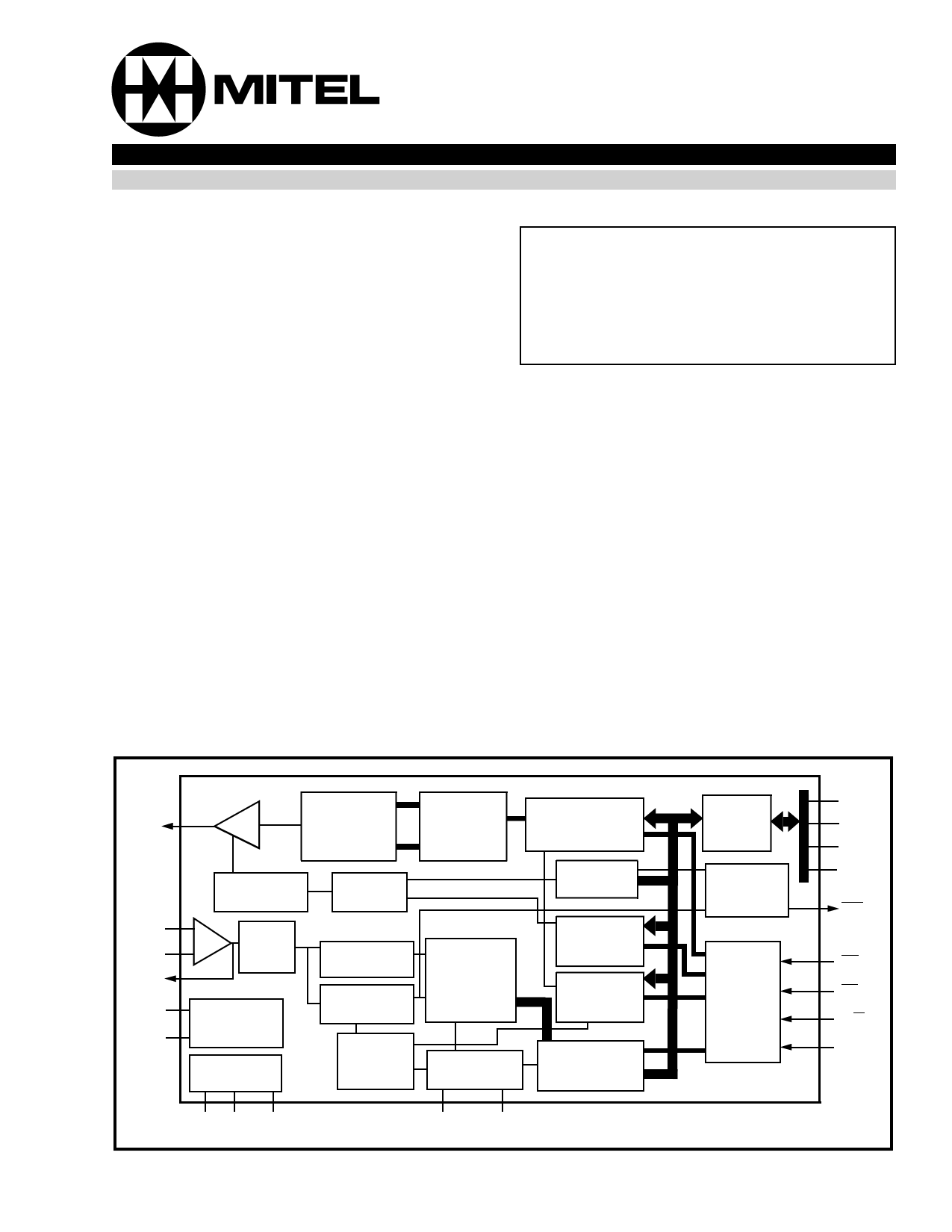
TONE
∑
D/A
Converters
IN+
IN-
GS
OSC1
OSC2
Tone Burst
Gating Cct.
+
Dial
-
Tone
Filter
Oscillator
Circuit
Bias
Circuit
Control
Logic
High Group
Filter
Low Group
Filter
Control
Logic
Row and
Column
Counters
Digital
Algorithm
and Code
Converter
Steering
Logic
Transmit Data
Register
Status
Register
Control
Register
A
Control
Register
B
Receive Data
Register
VDD VRef VSS
ESt
St/GT
Figure 1 - Functional Block Diagram
Data
Bus
Buffer
Interrupt
Logic
I/O
Control
D0
D1
D2
D3
IRQ/CP
RD
CS
R/W
RS0
4-91
Share Link: 