TC682CPA データシートの表示(PDF) - TelCom Semiconductor Inc => Microchip
部品番号
コンポーネント説明
メーカー
TC682CPA Datasheet PDF : 6 Pages
| |||
INVERTING VOLTAGE DOUBLER
1
TC682
DETAILED DESCRIPTION
Phase 1
VSS charge storage – before this phase of the clock
cycle, capacitor C1 is already charged to +5V. C1+ is then
switched to ground and the charge in C1– is transferred to C2–
. Since C2+ is at +5V, the voltage potential across capacitor
C2 is now –10V.
VIN = +5V
SW1
+
– C1
SW2
SW3
+
– C2
SW4
–5V
VOUT
–
+ C3
Figure 2. Charge Pump – Phase 1
Phase 2
VSS transfer – phase two of the clock connects the
negative terminal of C2 to the negative side of reservoir
capacitor C3 and the positive terminal of C2 to ground,
transferring the generated – 10V to C3. Simultaneously, the
positive side of capacitor C1 is switched to +5V and the
negative side is connected to ground. C2 is then switched to
VCC and GND and Phase 1 begins again.
+5V
SW1
+
– C1
SW2
SW3
+
– C2
SW4
–10V
VOUT
–
+ C3
Figure 3. Charge Pump – Phase 2
MAXIMUM OPERATING LIMITS
The TC682 has on-chip zener diodes that clamp VIN to
approximately 5.8V, and VO– UT to – 11.6V. Never exceed the
maximum supply voltage or excessive current will be shunted
by these diodes, potentially damaging the chip. The TC682
will operate over the entire operating temperature range with
an input voltage of 2V to 5.5V.
TELCOM SEMICONDUCTOR, INC.
EFFICIENCY CONSIDERATIONS
2 Theoretically a charge pump voltage multiplier can
approach 100% efficiency under the following conditions:
• The charge pump switches have virtually no offset
and are extremely low on resistance.
• Minimal power is consumed by the drive circuitry
• The impedances of the reservoir and pump capaci-
tors are negligible.
For the TC682, efficiency is as shown below:
3
Voltage Efficiency = VOUT / (– 2VIN)
VOUT = – 2VIN + VDROP
VDROP = (IOUT) (ROUT)
Power Loss
= IOUT (VDROP)
4 There will be a substantial voltage difference between
V–OUT and 2 VIN if the impedances of the pump capacitors
C1 and C2 are high with respect to their respective output
loads.
Larger values of reservoir capacitor C3 will reduce
output ripple. Larger values of both pump and reservoir
capacitors improve the efficiency. See "Capacitor Selec-
tion" in Applications section.
5
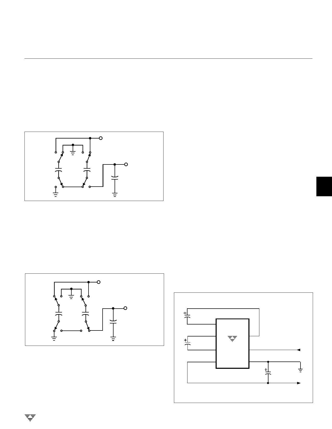
APPLICATIONS
Negative Doubling Converter
The most common application of the TC682 is as a
charge pump voltage converter which provides a negative
output of two times a positive input voltage (Figure 4).
6
C1
22µF
1 C1–
2 C2+
C1+ 7
C2
22µF
TC682
3 C2–
VIN 6
4 VO–UT
5
GND
C3
22µF
Figure 4. Inverting Voltage Doubler
VIN
7
GND
VO–UT
8
4-23
Share Link: 