AD9940 データシートの表示(PDF) - Analog Devices
部品番号
コンポーネント説明
メーカー
AD9940 Datasheet PDF : 20 Pages
| |||
AD9940
Data Sheet
ANALOG SPECIFICATIONS
fCLI = 56 MHz, AVDD = OVDD = DVDD = TCVDD = 3.0 V, −25°C to +85°C, unless otherwise noted.
Table 2.
Parameter
CDS
Gain
Allowable CCD Reset Transient1
Maximum Input Range Before Saturation1
Maximum CCD Black Pixel Amplitude1
Peak Nonlinearity, 500 mV Input Signal
Power Supply Rejection (PSR)
ANALOG OUTPUTS2
Typical DIFFP Output Signal Range
Typical DIFFN Output Signal Range
Typical Common Mode Level
Maximum Differential Output Voltage Swing
Output Voltage Compliance
Maximum Load Capacitance
Minimum Load Resistance (if required)
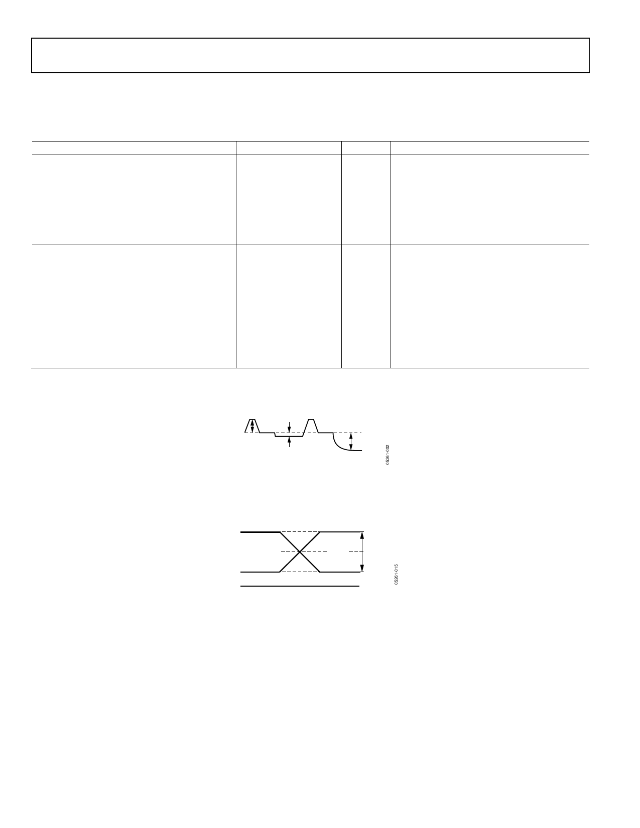
1 Input signal characteristics are defined in Figure 2.
2 Output signal characteristics are defined in Figure 3.
Min Typ Max
5.0 5.5 6.0
500
1
±50
0.2
36
1.2
2.2
1.2
2.2
1.7
2
1.0
2.4
24
5,000
Unit Notes
dB
mV
V p-p
mV
% FS
dB
Measured with step change on supply
V
1.2 V corresponds to black level
V
2.2 V corresponds to black level
V
Midscale voltage where DIFFP = DIFFN
V
Defined as DIFFP − DIFFN
V
Limitation of output swing into external load
pF
Value for each output (AD9941 CIN is < 24 pF)
Ω
Only use resistive loading if required by the
differential receiver. Proper dc biasing should
be used to be compatible with levels in Figure 3
500mV TYP
RESET TRANSIENT
50mV TYP
OPTICAL BLACK PIXEL
850mV TYP
INPUT SIGNAL RANGE
Figure 2. Input Signal Characteristics
1V MAX OUTPUT SIGNAL SWING, DIFFP AND DIFFN
2V p-p MAX DIFFERENTIAL SIGNAL, DIFFP–DIFFN
DIFFN
2.2V
BLACK
LEVEL
WHITE
LEVEL
1.7V
DIFFP
1.2V
GND
Figure 3. Output Signal Characteristics
Rev. A | Page 4 of 20
Share Link: 