ADUM1240 データシートの表示(PDF) - Analog Devices
部品番号
コンポーネント説明
メーカー
ADUM1240 Datasheet PDF : 24 Pages
| |||
Data Sheet
ADuM1240/ADuM1241/ADuM1245/ADuM1246
SPECIFICATIONS
ELECTRICAL CHARACTERISTICS—3.3 V OPERATION
All typical specifications are at TA = 25°C, VDD1 = VDD2 = 3.3 V. Minimum and maximum specifications apply over the entire
recommended operation range of 3.0 V ≤ VDD1 ≤ 3.6 V, 3.0 V ≤ VDD2 ≤ 3.6 V, and −40°C ≤ TA ≤ +125°C, unless otherwise noted. Switching
specifications are tested with CL = 15 pF and CMOS signal levels, unless otherwise noted.
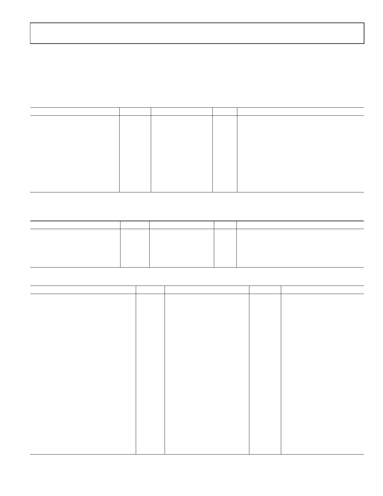
Table 1.
Parameter
SWITCHING SPECIFICATIONS
Data Rate
Propagation Delay
Change vs. Temperature
Minimum Pulse Width
Pulse Width Distortion
Propagation Delay Skew1
Channel Matching
Codirectional
Opposing Direction
Symbol
tPHL, tPLH
PW
PWD
tPSK
tPSKCD
tPSKOD
Min Typ Max Unit Test Conditions/Comments
2
80 180
200
500
8
10
Mbps
ns
ps/°C
ns
ns
ns
Within pulse width distortion (PWD) limit
50% input to 50% output
Within PWD limit
|tPLH − tPHL|
10
ns
15
ns
1 tPSK is the magnitude of the worst case difference in tPHL and tPLH that is measured between units at the same operating temperature, supply voltages, and output load within the
recommended operating conditions.
Table 2.
Parameter
SUPPLY CURRENT
ADuM1240/ADuM1245
ADuM1241/ADuM1246
Symbol Min
IDD1
IDD2
IDD1
IDD2
Typ Max
366 600
246 375
306 450
306 450
Unit
µA
µA
µA
µA
Test Conditions/Comments
2 Mbps, no load
Table 3.
Parameter
DC SPECIFICATIONS
Input Threshold
Logic High
Logic Low
Output Voltages
Logic High
Logic Low
Input Current per Channel
Input Switching Thresholds
Positive Threshold Voltage
Negative Going Threshold
Input Hysteresis
Undervoltage Lockout, VDD1 or VDD2
Supply Current per Channel
Quiescent Current
Input Supply
Output Supply
Input (Refresh Off )
Output (Refresh Off )
Symbol Min
Typ Max
Unit
VIH
VIL
VOH
VOL
II
VT+
VT−
ΔVT
UVLO
0.7 VDDx1
V
0.3 VDDx1 V
VDDx1 − 0.1 3.3
V
VDDx1 − 0.4
3.1
V
0.0
0.1
V
0.2
0.4
V
−1
+0.01 +1
µA
1.8
V
1.2
V
0.6
V
1.5
V
IDDI (Q)
IDDO (Q)
IDDI (Q)
IDDO (Q)
4.8
10
µA
0.8
6
µA
0.12
µA
0.13
µA
Test Conditions/Comments
IOUTx = −20 µA, VIx = VIxH
IOUTx = −4 mA, VIx = VIxH
IOUTx = 20 µA, VIx = VIxL
IOUTx = 4 mA, VIx = VIxL
0 V ≤ VIx ≤ VDDx1
ENX low
ENX low
ENX high
ENX high
Rev. B | Page 3 of 24
Share Link: 