DMC3035LSD データシートの表示(PDF) - Diodes Incorporated.
部品番号
コンポーネント説明
メーカー
DMC3035LSD Datasheet PDF : 7 Pages
| |||
Not Recommended for New Design,
Use DMC3036LSD-13
DMC3035LSD
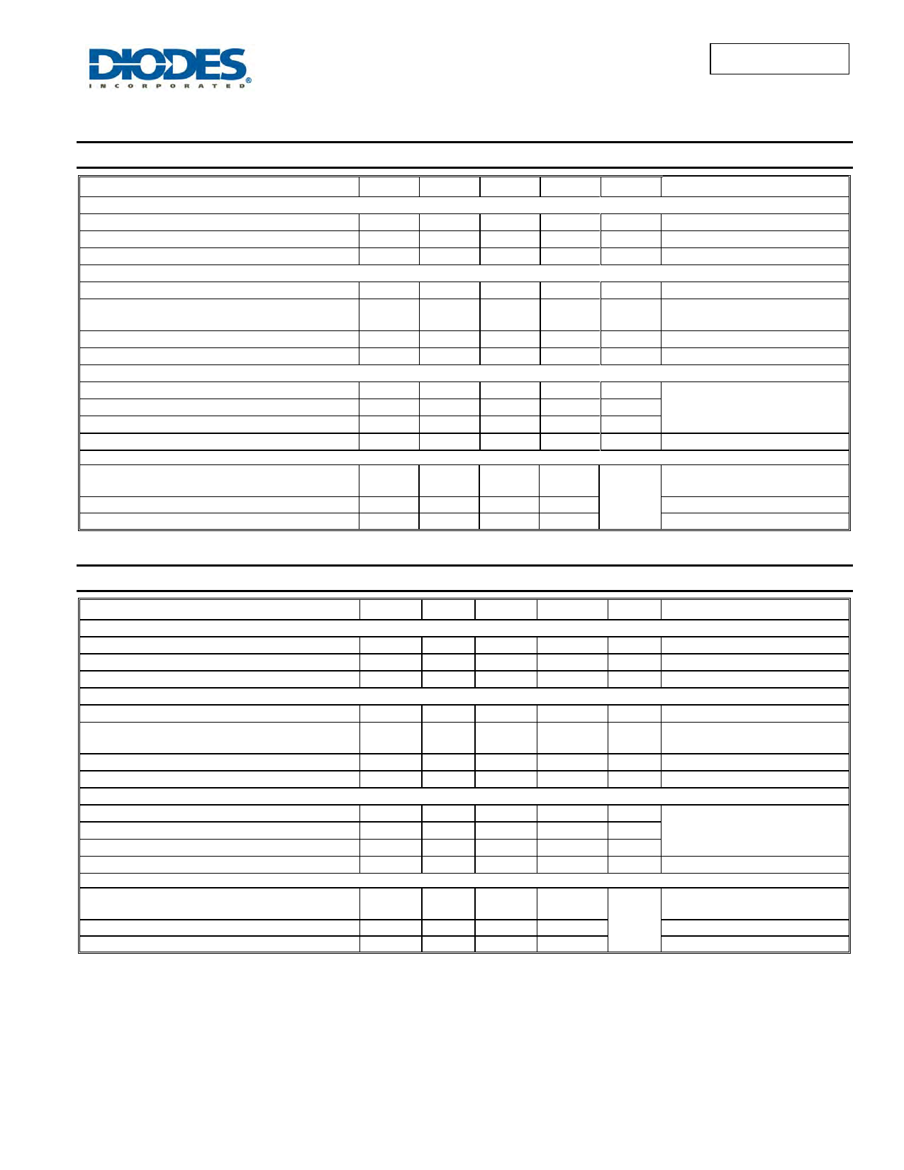
Electrical Characteristics N-CHANNEL @TA = 25°C unless otherwise specified
Characteristic
OFF CHARACTERISTICS (Note 5)
Drain-Source Breakdown Voltage
Zero Gate Voltage Drain Current
Gate-Source Leakage
ON CHARACTERISTICS (Note 5)
Gate Threshold Voltage
Static Drain-Source On-Resistance
Forward Transfer Admittance
Diode Forward Voltage (Note 5)
DYNAMIC CHARACTERISTICS
Input Capacitance
Output Capacitance
Reverse Transfer Capacitance
Gate Resistance
SWITCHING CHARACTERISTICS
Total Gate Charge
Gate-Source Charge
Gate-Drain Charge
Symbol Min
BVDSS
30
IDSS
⎯
IGSS
⎯
VGS(th)
1
RDS (ON)
⎯
⎯
|Yfs|
⎯
VSD
0.5
Ciss
⎯
Coss
⎯
Crss
⎯
RG
⎯
Qg
⎯
Qgs
⎯
Qgd
⎯
Typ
Max
Unit
⎯
⎯
V
⎯
1
μA
⎯
± 100
nA
⎯
2.1
V
28
51
35
61
mΩ
7.7
⎯
S
⎯
1.2
V
384
⎯
pF
67
⎯
pF
48
⎯
pF
1.3
⎯
Ω
4.3
8.6
⎯
1.2
⎯
nC
2.5
⎯
Test Condition
VGS = 0V, ID = 250μA
VDS = 24V, VGS = 0V
VGS = ±20V, VDS = 0V
VDS = VGS, ID = 250μA
VGS = 10V, ID = 6.9A
VGS = 4.5V, ID = 5.0A
VDS = 5V, ID = 6.9A
VGS = 0V, IS = 1A
VDS = 15V, VGS = 0V, f = 1.0MHz
VGS = 0V, VDS = 0V, f = 1MHz
VDS = 10V, VGS = 4.5V, ID = 10A
VDS = 10V, VGS = 10V, ID = 10A
VDS = 10V, VGS = 10V, ID = 10A
VDS = 10V, VGS = 10V, ID = 10A
Electrical Characteristics P-CHANNEL @TA = 25°C unless otherwise specified
Characteristic
Symbol Min
Typ
OFF CHARACTERISTICS (Note 5)
Drain-Source Breakdown Voltage
Zero Gate Voltage Drain Current
Gate-Source Leakage
ON CHARACTERISTICS (Note 5)
BVDSS
-30
⎯
IDSS
⎯
⎯
IGSS
⎯
⎯
Gate Threshold Voltage
Static Drain-Source On-Resistance
VGS(th)
-1
⎯
RDS (ON)
⎯
⎯
56
98
Forward Transfer Admittance
Diode Forward Voltage (Note 5)
DYNAMIC CHARACTERISTICS
Input Capacitance
Output Capacitance
Reverse Transfer Capacitance
Gate Resistance
SWITCHING CHARACTERISTICS
|Yfs|
⎯
⎯
VSD
-0.5
⎯
Ciss
⎯
336
Coss
⎯
70
Crss
⎯
49
RG
⎯
4.6
Total Gate Charge
Qg
⎯
4.0
7.8
Gate-Source Charge
Gate-Drain Charge
Qgs
⎯
1.0
Qgd
⎯
2.5
Notes: 5. Short duration pulse test used to minimize self-heating effect.
Max
⎯
-1.0
± 100
-2.1
65
115
5.2
-1.2
⎯
⎯
⎯
⎯
⎯
⎯
⎯
Unit
Test Condition
V VGS = 0V, ID = -250μA
μA VDS = -24V, VGS = 0V
nA VGS = ±20V, VDS = 0V
V VDS = VGS, ID = -250μA
mΩ
VGS = -10V, ID = -5A
VGS = -4.5V, ID = -4A
S VDS = -10V, ID = -5A
V VGS = 0V, IS = -2.6A
pF
pF VDS = -25V, VGS = 0V, f = 1.0MHz
pF
Ω VGS = 0V, VDS = 0V, f = 1MHz
VDS = 15V, VGS = -4.5V, ID = -5A
nC VDS = 15V, VGS = -10V, ID = -5A
VDS = 15V, VGS = -10V, ID = -5A
VDS = 15V, VGS = -10V, ID = -5A
DMC3035LSD
Document number: DS31312 Rev. 5 - 3
2 of 7
www.diodes.com
July 2011
© Diodes Incorporated
Share Link: 