AD7883BN データシートの表示(PDF) - Analog Devices
部品番号
コンポーネント説明
メーカー
AD7883BN Datasheet PDF : 12 Pages
| |||
AD7883
APPLICATION HINTS
Good printed circuit board (PCB) layout is as important as the
circuit design itself in achieving high speed A/D performance.
The AD7883’s comparator is required to make bit decisions on
an LSB size of 0.8 mV. To achieve this, the designer must be
conscious of noise both in the ADC itself and in the preceding
analog circuitry. Switching mode power supplies are not recom-
mended, as the switching spikes will feed through to the com-
parator causing noisy code transitions. Other causes of concern
are ground loops and digital feedthrough from microprocessors.
These are factors which influence any ADC, and a proper
PCB layout which minimizes these effects is essential for best
performance.
LAYOUT HINTS
Ensure that the layout for the printed circuit board has the digi-
tal and analog signal lines separated as much as possible. Take
care not to run digital tracks alongside analog signal tracks.
Guard (screen) the analog input with AGND.
Establish a single point analog ground (star ground) separate
from the logic system ground at the AD7883 AGND pin or as
close as possible to the AD7883. Connect all other grounds and
the AD7883 DGND to this single analog ground point. Do not
connect any other digital grounds to this analog ground point.
Low impedance analog and digital power supply common re-
turns are essential to low noise operation of the ADC, so make
the foil width for these tracks as wide as possible. The use of
ground planes minimizes impedance paths and also guards the
analog circuitry from digital noise.
NOISE
Keep the input signal leads to VIN and signal return leads from
AGND as short as possible to minimize input noise coupling. In
applications where this is not possible, use a shielded cable be-
tween the source and the ADC. Reduce the ground circuit im-
pedance as much as possible since any potential difference in
grounds between the signal source and the ADC appears as an
error voltage in series with the input signal.
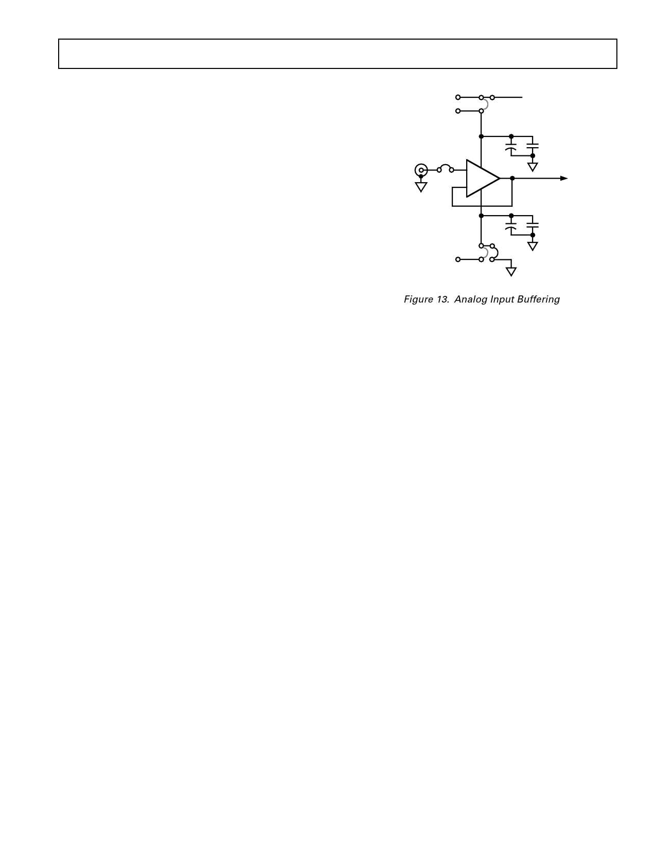
LK2
AB
V+
VDD
V+
ANALOG
INPUT LK1
SKT1
C1
10µF
V+
+
IC1
–
V–
C2
0.1µF
TO ADC
C3
10µF
C4
0.1µF
V–
AB
LK3
Figure 13. Analog Input Buffering
ANALOG INPUT BUFFERING
To achieve specified performance, it is recommended that the
analog input (VINA, VINB) be driven from a low impedance
source. This necessitates the use of an input buffer amplifier.
The choice of op amp will be a function of the particular appli-
cation and the desired analog input range.
The simplest configuration is the 0 V to VREF range of Figure 4.
A single supply op amp is recommended for such an implemen-
tation. This will allow for operation of the AD7883 in the 0 to
VREF unipolar range without supplying an external supply to V+
and V– of the op amp. Recommended single-supply op amps
are the OP-195 and AD820.
In bipolar operation, positive and negative supplies must be
connected to V+ and V– of the op amp.
The AD711 is a general purpose op amp which could be used
to drive the analog input of the AD7883, in this input range.
REV. 0
–9–
Share Link: 