ML4876 データシートの表示(PDF) - Micro Linear Corporation
部品番号
コンポーネント説明
メーカー
ML4876 Datasheet PDF : 9 Pages
| |||
ML4876
FUNCTIONAL DESCRIPTION (Continued)
CONTRAST CONTROL GENERATOR
The contrast voltage generator is a separate regulator in a
flyback configuration. In conjunction with the external
transformer (T3), MOSFET (Q1), diode (D1), and assorted
capacitors and resistors, it provides an adjustable DC
output contrast voltage necessary to drive LCD screens.
The voltage is adjusted by controlling the voltage applied
to R5 at the contrast adjustment point.
The contrast voltage can be made either positive or
negative simply by changing the connection of the
external components. The schematic shown in Figure 1 is
connected for a negative voltage. Please refer to
Application Note 32 for the circuit connection for a
positive output voltage.
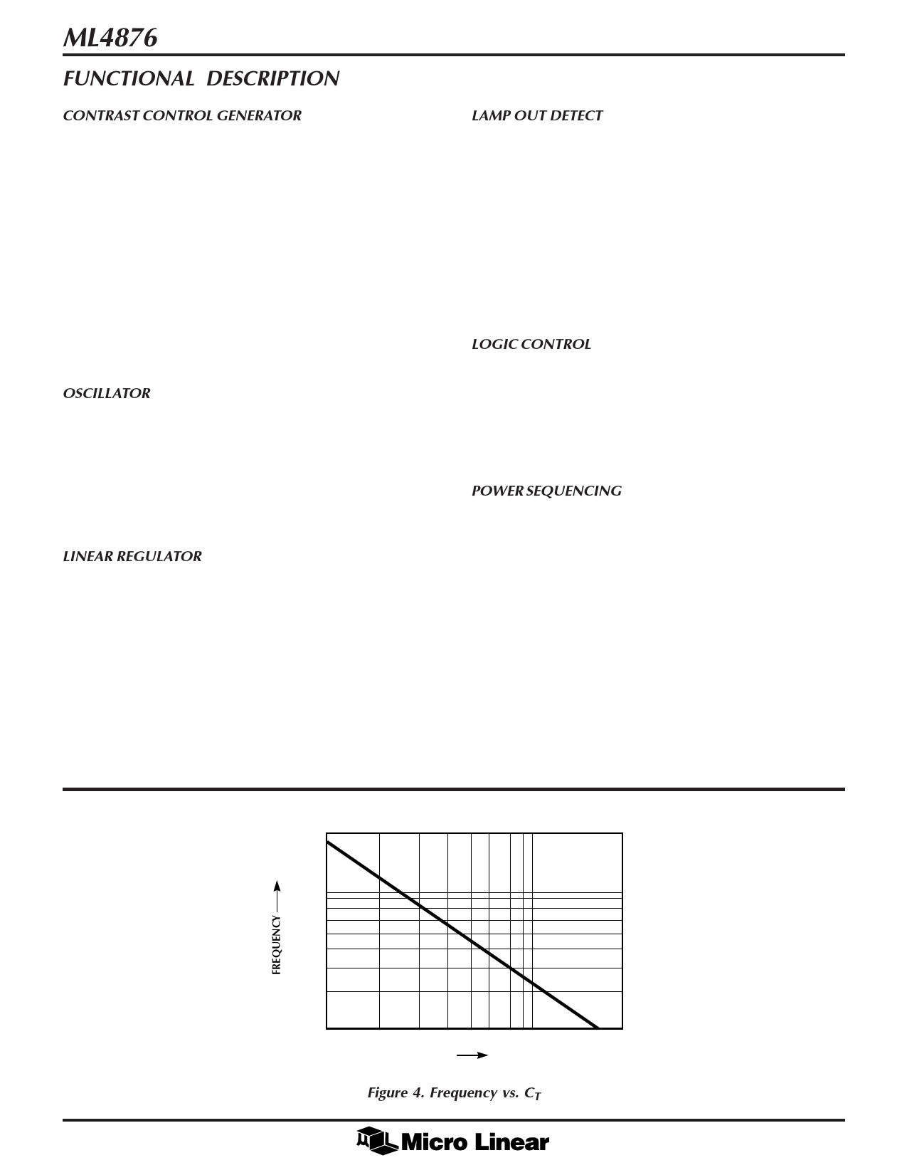
OSCILLATOR
The frequency of the oscillator in the ML4876 is set by
selecting the value of CT.
Figure 4 shows the oscillator frequency versus the value
of CT. This nomograph may be used to select the
appropriate value of CT to achieve the desired oscillator
frequency.
LINEAR REGULATOR
A linear voltage regulator is provided to power the low
voltage and low current control circuitry on the ML4876.
This is typically used when there is no separate 5V supply
available at the inverter board. For operation up to 18V
the linear regulator is used by connecting HVDD to the
input battery voltage. For operation over 18V, a MOSFET
and a resistor (Q2 and R1, Figure 1) are connected as
shown. The MOSFET is required to stand off the high
voltage.
LAMP OUT DETECT
In those cases when there is no lamp connected, or the
connection is faulty, the output voltage of the lamp driver
circuit will tend to rise to a high level in an attempt to
start the nonexistent lamp. The lamp out detect circuit on
the ML4876 will detect this condition by sensing the
center tap voltage on the primary of the output
transformer (T1) on the L RTD pin. When this voltage
exceeds 16V, an internal latch is set and the lamp driver
goes into a shutdown mode. The logic control pin L ON
must be cycled low, then high to reset the latch and
return the lamp driver to the normal state.
LOGIC CONTROL
The ML4876 is controlled by a two logic inputs, L ON and
ON/OFF. A logic level high on the L ON pin enables just
the lamp driver. A logic zero on the L ON pin disable the
lamp driver only. A logic level high on the ON/OFF pin
enable the complete circuit. A logic level low on the
ON/OFF pin puts the circuit into a very low power state.
POWER SEQUENCING
It is important to observe correct power and logic input
sequencing when powering up the ML4876. The following
procedure must be observed to avoid damaging the
device.
1. Apply the battery power to HVDD
2. Apply the VDD voltage (if HVDD is not used). With
HVDD connected this voltage is supplied by the
internal regulator on the ML4876.
3. Apply a logic high to the ON/OFF input. This will
enable the internal linear regulator to ensure the VDD
supply is on (when HVDD is used).
4. Apply a logic high to the L ON input.
200KHz
100KHz
70KHz
50KHz
40KHz
30KHz
20pF
30pF
40pF 50pF
CT
70pF
100pF
Figure 4. Frequency vs. CT
200pF
8
Share Link: 