SST25VF032B データシートの表示(PDF) - Microchip Technology
部品番号
コンポーネント説明
メーカー
SST25VF032B Datasheet PDF : 33 Pages
| |||
A Microchip Technology Company
32 Mbit SPI Serial Flash
SST25VF032B
High-Speed-Read (80 MHz)
Data Sheet
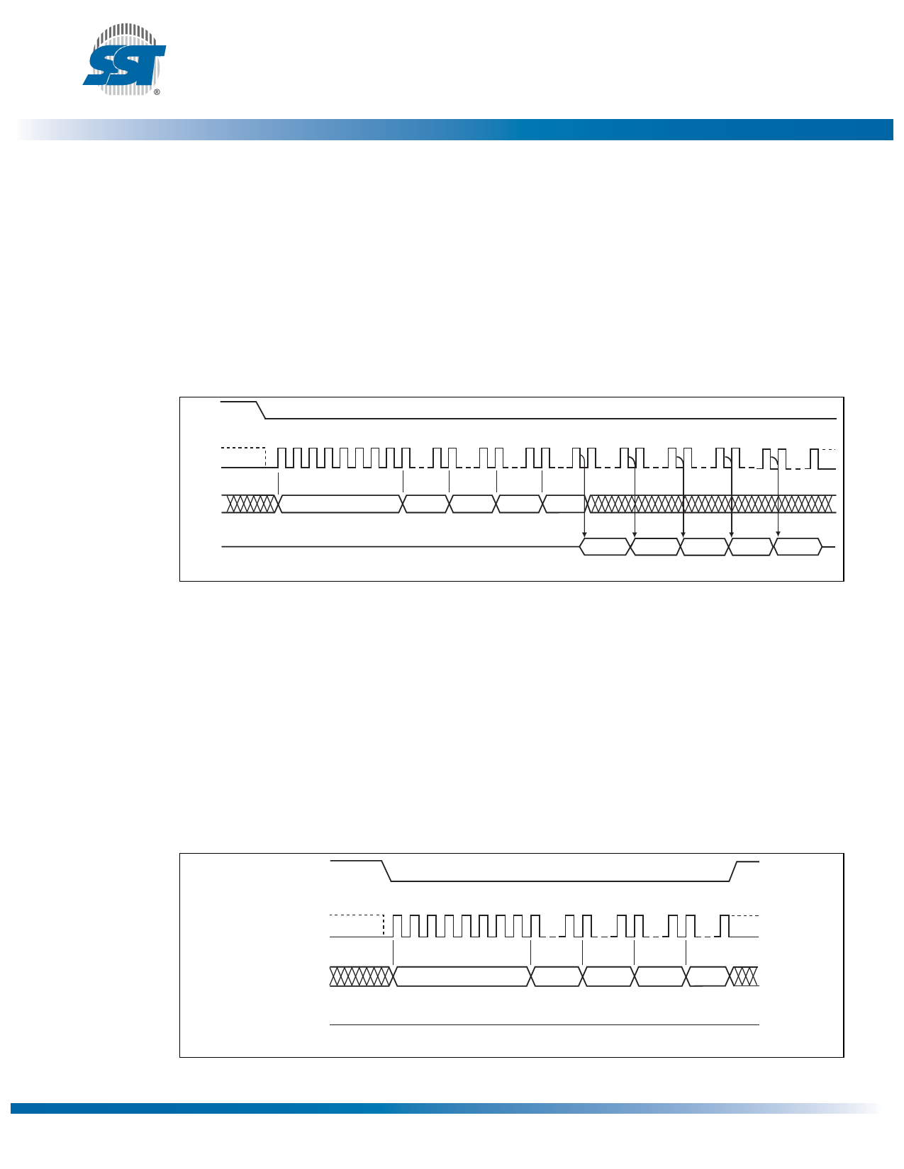
The High-Speed-Read instruction supporting up to 80 MHz Read is initiated by executing an 8-bit com-
mand, 0BH, followed by address bits [A23-A0] and a dummy byte. CE# must remain active low for the
duration of the High-Speed-Read cycle. See Figure 6 for the High-Speed-Read sequence.
Following a dummy cycle, the High-Speed-Read instruction outputs the data starting from the specified
address location. The data output stream is continuous through all addresses until terminated by a low to
high transition on CE#. The internal address pointer will automatically increment until the highest memory
address is reached. Once the highest memory address is reached, the address pointer will automatically
increment to the beginning (wrap-around) of the address space. For example, once the data from address
location 3FFFFFH has been read, the next output will be from address location 000000H.
CE#
MODE 3 0 1 2 3 4 5 6 7 8 15 16 23 24 31 32 39 40 47 48 55 56 63 64 71 72 78
SCK MODE 0
SI
0B
ADD. ADD. ADD.
SO
HIGH IMPEDANCE
Figure 6: High-Speed-Read Sequence
X
N
DOUT
MSB
N+1
DOUT
N+2
DOUT
N+3
DOUT
N+4
DOUT
1327 F07.1
Byte-Program
The Byte-Program instruction programs the bits in the selected byte to the desired data. The selected
byte must be in the erased state (FFH) when initiating a Program operation. A Byte-Program instruction
applied to a protected memory area will be ignored.
Prior to any Write operation, the Write-Enable (WREN) instruction must be executed. CE# must remain
active low for the duration of the Byte-Program instruction. The Byte-Program instruction is initiated by
executing an 8-bit command, 02H, followed by address bits [A23-A0]. Following the address, the data is
input in order from MSB (bit 7) to LSB (bit 0). CE# must be driven high before the instruction is exe-
cuted. The user may poll the Busy bit in the software status register or wait TBP for the completion of
the internal self-timed Byte-Program operation. See Figure 7 for the Byte-Program sequence.
CE#
SCK
MODE 3
MODE 0
012 345 6 78
15 16
23 24 31 32 39
SI
02
SO
Figure 7: Byte-Program Sequence
ADD.
ADD.
ADD.
DIN
MSB LSB
HIGH IMPEDANCE
1327 F08.0
©2011 Silicon Storage Technology, Inc.
11
DS25071A
12/11
Share Link: 