SST49LF008A データシートの表示(PDF) - Microchip Technology
部品番号
コンポーネント説明
メーカー
SST49LF008A Datasheet PDF : 45 Pages
| |||
A Microchip Technology Company
8 Mbit Firmware Hub
SST49LF008A
Data Sheet
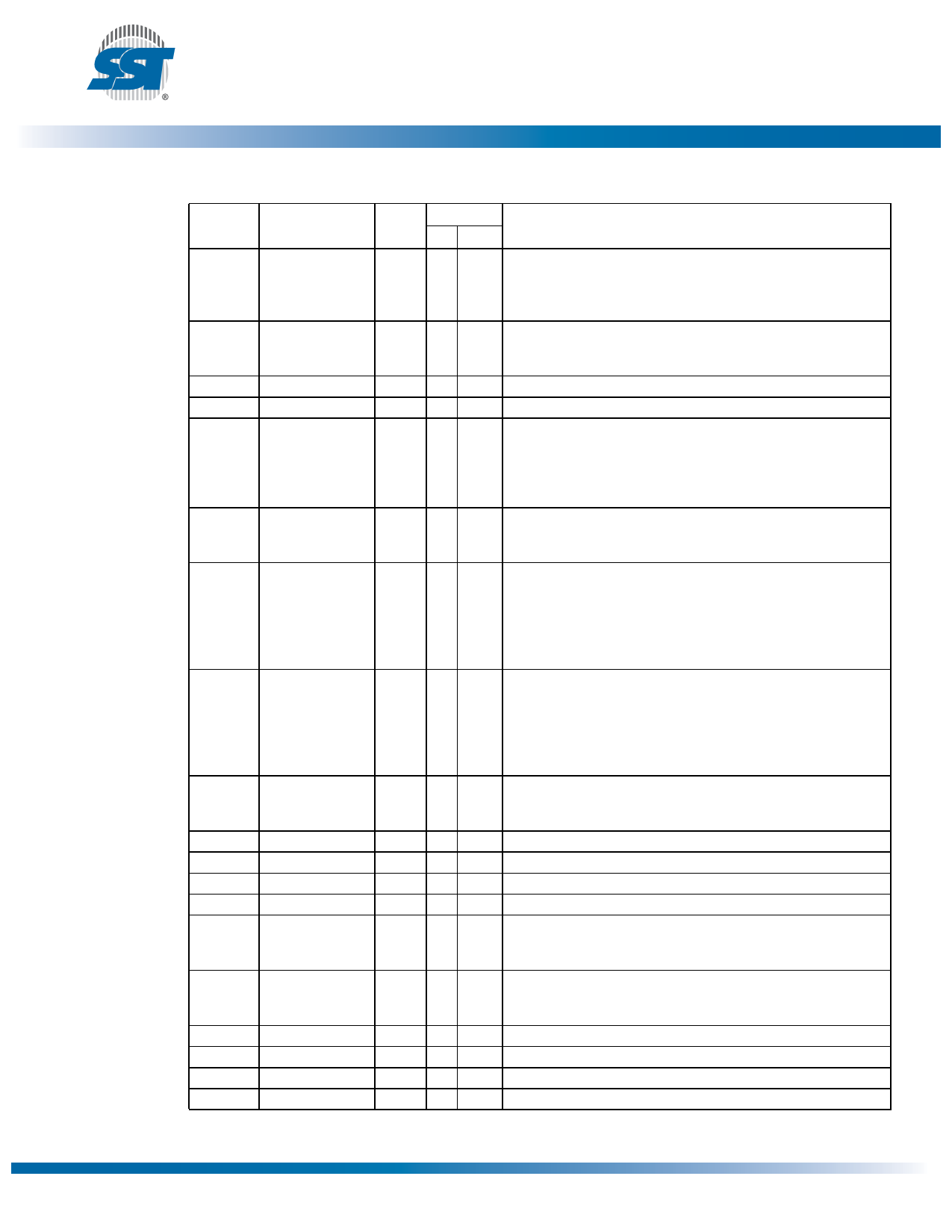
Table 1: Pin Description
Symbol Pin Name
A10-A0 Address
DQ7-DQ0 Data
OE#
WE#
IC
Output Enable
Write Enable
Interface
Configuration
Pin
INIT# Initialize
ID[3:0]
Identification
Inputs
FGPI[4:0] General Pur-
pose Inputs
TBL#
Top Block Lock
FWH[3:0] FWH I/Os
CLK
Clock
FWH4 FWH Input
RST# Reset
WP#
Write Protect
R/C#
Row/Column
Select
RES
VDD
VSS
NC
Reserved
Power Supply
Ground
No Connection
1. I = Input, O = Output
Interface
Type1 PP FWH Functions
IX
Inputs for low-order addresses during Read and Write opera-
tions. Addresses are internally latched during a Write cycle. For
the programming interface, these addresses are latched by R/
C# and share the same pins as the high-order address inputs.
I/O X
To output data during Read cycles and receive input data during
Write cycles. Data is internally latched during a Write cycle. The
outputs are in tri-state when OE# is high.
IX
To gate the data output buffers
IX
To control the Write operations
I X X This pin determines which interface is operational. When held
high, programmer mode is enabled and when held low, FWH
mode is enabled. This pin must be setup at power-up or before
return from reset and not change during device operation. This pin
is internally pulled- down with a resistor between 20-100 K
I
X This is the second reset pin for in-system use. This pin is inter-
nally combined with the RST# pin; If this pin or RST# pin is
driven low, identical operation is exhibited.
I
X These four pins are part of the mechanism that allows multiple
parts to be attached to the same bus. The strapping of these
pins is used to identify the component.The boot device must
have ID[3:0]=0000 and it is recommended that all subsequent
devices should use sequential up-count strapping. These pins
are internally pulled-down with a resistor between 20-100 K
I
X These individual inputs can be used for additional board flexibil-
ity. The state of these pins can be read through GPI_REG regis-
ter. These inputs should be at their desired state before the start
of the PCI clock cycle during which the read is attempted, and
should remain in place until the end of the Read cycle. Unused
GPI pins must not be floated.
I
X When low, prevents programming to the Boot Block sectors at top of
memory. When TBL# is high it disables hardware write protection for
the top block sectors. This pin cannot be left unconnected.
I/O
X I/O Communications
I
X To provide a clock input to the control unit
I
X Input Communications
I X X To reset the operation of the device
I
X When low, prevents programming to all but the highest address-
able blocks. When WP# is high it disables hardware write protec-
tion for these blocks. This pin cannot be left unconnected.
IX
Select For the Programming interface, this pin determines whether
the address pins are pointing to the row addresses, or to the column
addresses.
X These pins must be left unconnected.
PWR X X To provide power supply (3.0-3.6V)
PWR X
IX
X Circuit ground (OV reference) All VSS pins must be grounded.
X Unconnected pins
T1.4 25085
©2011 Silicon Storage Technology, Inc.
6
DS25085A
10/11
Share Link: 