HA-5002-5(1998) データシートの表示(PDF) - Intersil
部品番号
コンポーネント説明
メーカー
HA-5002-5 Datasheet PDF : 13 Pages
| |||
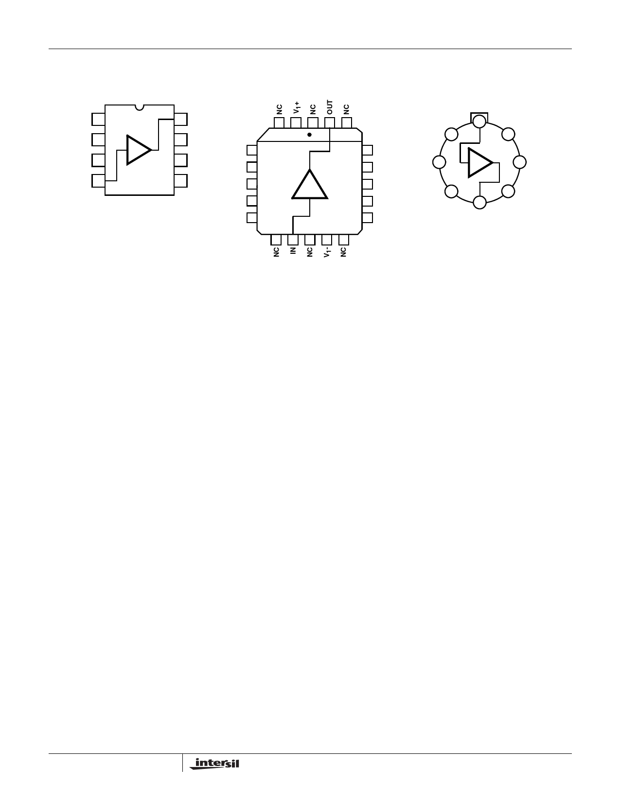
HA-5002
Absolute Maximum Ratings
Voltage Between V+ and V- Terminals. . . . . . . . . . . . . . . . . . . . 44V
Input Voltage . . . . . . . . . . . . . . . . . . . . . . . . . . . . . . . . . . V1+ to V1-
Output Current (Continuous) . . . . . . . . . . . . . . . . . . . . . . . . ±200mA
Output Current (50ms On, 1s Off) . . . . . . . . . . . . . . . . . . . . ±400mA
Operating Conditions
Temperature Range
HA-5002-2 . . . . . . . . . . . . . . . . . . . . . . . . . . . . . . -55oC to 125oC
HA-5002-5 . . . . . . . . . . . . . . . . . . . . . . . . . . . . . . . . 0oC to 75oC
HA-5002-9 . . . . . . . . . . . . . . . . . . . . . . . . . . . . . . . -40oC to 85oC
Thermal Information
Thermal Resistance (Typical, Note 2) θJA (oC/W)θJC (oC/W)
CERDIP Package. . . . . . . . . . . . . . . . . 115
28
PDIP Package . . . . . . . . . . . . . . . . . . .
92
N/A
Metal Can Package . . . . . . . . . . . . . . . 155
67
PLCC Package. . . . . . . . . . . . . . . . . . .
74
N/A
SOIC Package . . . . . . . . . . . . . . . . . . . 157
N/A
Max Junction Temperature (Hermetic Packages, Note 1) . . . . . . 175oC
Max Junction Temperature (Plastic Packages, Note 1) . . . . . . . . 150oC
Max Storage Temperature Range . . . . . . . . . . . . . . -65oC to 150oC
Max Lead Temperature (Soldering 10s) . . . . . . . . . . . . . . . . 300oC
(PLCC and SOIC - Lead Tips Only)
CAUTION: Stresses above those listed in “Absolute Maximum Ratings” may cause permanent damage to the device. This is a stress only rating and operation of the
device at these or any other conditions above those indicated in the operational sections of this specification is not implied.
NOTES:
1. Maximum power dissipation, including load conditions, must be designed to maintain the maximum junction temperature below 175oC for the
ceramic and can packages, and below 150oC for the plastic packages.
2. θJA is measured with the component mounted on an evaluation PC board in free air.
Electrical Specifications VSUPPLY = ±12V to ±15V, RS = 50Ω, RL = 1kΩ, CL = 10pF, Unless Otherwise Specified
PARAMETER
TEST
CONDITIONS
TEMP
(oC)
HA-5002-2
MIN
TYP
MAX
HA-5002-5, -9
MIN
TYP
MAX
INPUT CHARACTERISTICS
Offset Voltage
25
-
5
20
-
5
20
Full
-
10
30
-
10
30
Average Offset Voltage Drift
Full
-
30
-
-
30
-
Bias Current
25
-
2
7
-
2
7
Full
-
3.4
10
-
2.4
10
Input Resistance
Full
1.5
3
-
1.5
3
-
Input Noise Voltage
10Hz-1MHz
25
-
18
-
-
18
-
TRANSFER CHARACTERISTICS
Voltage Gain
(VOUT = ±10V)
-3dB Bandwidth
AC Current Gain
RL = 50Ω
RL = 100Ω
RL = 1kΩ
RL = 1kΩ
VIN = 1VP-P
25
-
0.900
-
-
0.900
-
25
-
0.971
-
-
0.971
-
25
-
0.995
-
-
0.995
-
Full 0.980
-
-
0.980
-
-
25
-
110
-
-
110
-
25
-
40
-
-
40
-
OUTPUT CHARACTERISTICS
Output Voltage Swing
Output Current
Output Resistance
RL = 100Ω
25
±10
±10.7
-
RL = 1kΩ, VS = ±15V
Full
±10
±13.5
-
RL = 1kΩ, VS = ±12V
Full
±10
±10.5
-
VIN = ±10V, RL = 40Ω
25
-
220
-
Full
-
3
10
±10
±11.2
-
±10
±13.9
-
±10
±10.5
-
-
220
-
-
3
10
Harmonic Distortion
TRANSIENT RESPONSE
VIN = 1VRMS, f = 10kHz
25
-
<0.005
-
-
<0.005
-
Full Power Bandwidth (Note 3)
25
-
20.7
-
-
20.7
-
Rise Time
25
-
3.6
-
-
3.6
-
Propagation Delay
25
-
2
-
-
2
-
Overshoot
25
-
30
-
-
30
-
Slew Rate
25
1.0
1.3
-
1.0
1.3
-
Settling Time
To 0.1%
25
-
50
-
-
50
-
Differential Gain
Differential Phase
RL = 500Ω
RL = 500Ω
25
-
0.06
-
25
-
0.22
-
-
0.06
-
-
0.22
-
UNITS
mV
mV
µV/οC
µA
µA
MΩ
µVP-P
V/V
V/V
V/V
V/V
MHz
A/mA
V
V
V
mA
Ω
%
MHz
ns
ns
%
V/ns
ns
%
Degrees
2
Share Link: 