MAX14515 データシートの表示(PDF) - Maxim Integrated
部品番号
コンポーネント説明
メーカー
MAX14515 Datasheet PDF : 15 Pages
| |||
High-Voltage Liquid Lens Driver
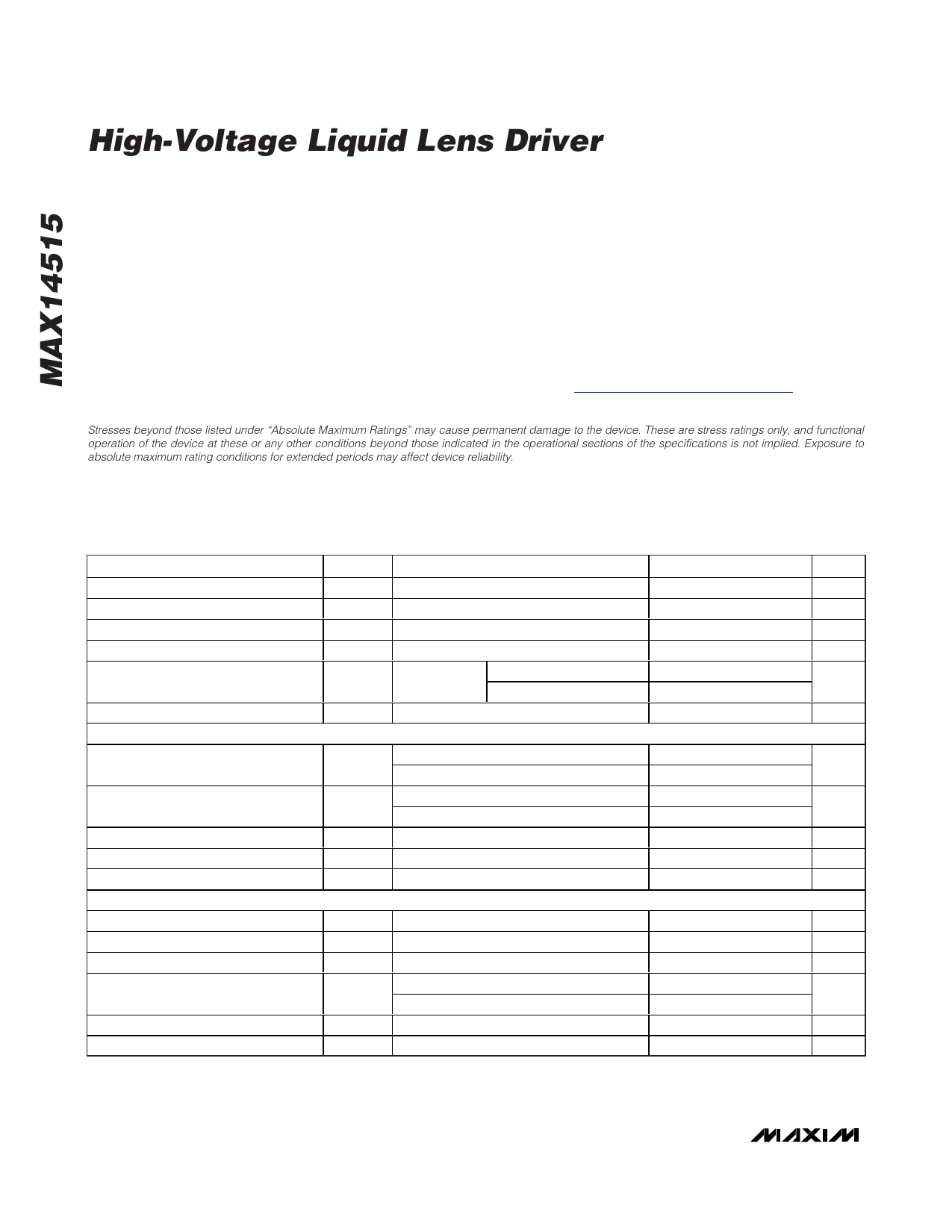
ABSOLUTE MAXIMUM RATINGS
(All voltages referenced to GND.)
VDD ........................................................................-0.3V to +6.0V
VA, VB .....................................................................-0.3V to +52V
VREF.........................................MAX (-0.3V, VDD - 0.3V) to +6.0V
SDA, SCL, EN........................................................-0.3V to +6.0V
Continuous Power Dissipation (TA = +70°C):
8-Bump WLP (derate 5.2mW/°C above +70°C)...........416mW
Junction-to-Ambient Thermal Resistance (qJA) (Note 1)
8-Bump WLP ..............................................................192°C/W
Operating Temperature Range ...........................-40°C to +85°C
Junction Temperature ......................................................+150°C
Storage Temperature Range .............................-65°C to +150°C
Lead Temperature (soldering, 10s) .................................+300°C
Note 1: Package thermal resistances were obtained using the method described in JEDEC specification JESD51-7, using a four-layer
board. For detailed information on package thermal considerations, refer to www.maxim-ic.com/thermal-tutorial.
Stresses beyond those listed under “Absolute Maximum Ratings” may cause permanent damage to the device. These are stress ratings only, and functional
operation of the device at these or any other conditions beyond those indicated in the operational sections of the specifications is not implied. Exposure to
absolute maximum rating conditions for extended periods may affect device reliability.
ELECTRICAL CHARACTERISTICS
(VDD = +2.7V to +5.5V, CVDD = 0.1µF, CREF = 1µF, CLENS = 220pF, TA = -40°C to +85°C, unless otherwise noted. Typical values are at
VDD = +2.8V and TA = +25°C.) (Note 2)
PARAMETER
Input Voltage
Input Supply Current
Reference Output Voltage
Shutdown Supply Current
Sleep Supply Current
POR Threshold
HIGH-VOLTAGE OUTPUTS (VA, VB)
Peak Output Voltage (Note 3)
Output RMS Voltage
Output Voltage Ripple
Pulldown Strength
Output Switching Frequency
CONTROL INPUTS (SDA, SCL, EN)
Input Logic-High Voltage
Input Logic-Low Voltage
Output Logic-Low Voltage
Input Low Leakage Current
Input High Leakage Current
Input Capacitance
SYMBOL
CONDITIONS
VDD
IDD
VREF
Peak output voltage register (VP) = 0xFF
ISHDN
ISLEEP
EN = GND
SM = 0,
SDA = SCL
VTH_POR
VEN = 1.8V, VDD = 4.2V
VEN = VDD, VDD = 2.8V
VPEAK
VRMS
VRPL
RLPD
fLENS
VP = 0x01
VP = 0xFF
VP = 0x01
VP = 0xFF
CLENS = 120pF
SM = 0
VIH
VIL
VOL ISINK = 3mA
IIL
EN = VCC
EN = GND
IIH
CIN
MIN TYP MAX UNITS
2.7
5.5
V
9
mA
5.5
V
1
500
nA
8
µA
1.2
3
2.6
V
10
V
52
10
V
42
47
±250
mV
2
kΩ
1
1.1
1.2
kHz
1.5
V
0.5
V
0.4
V
0.01
6
µA
0.01 0.5
0.01 2.5
µA
10
pF
2 _______________________________________________________________________________________
Share Link: 