KSZ8041FTL データシートの表示(PDF) - Micrel
部品番号
コンポーネント説明
メーカー
KSZ8041FTL Datasheet PDF : 58 Pages
| |||
Micrel, Inc.
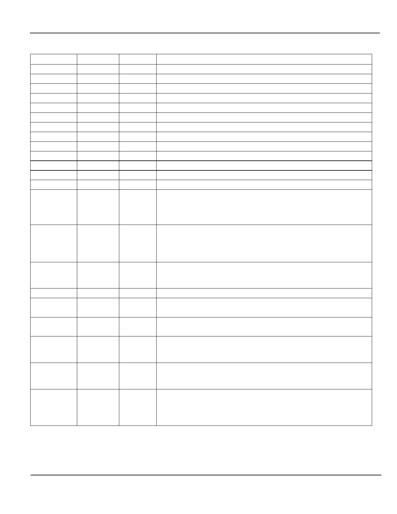
Pin Description
Pin Number
1
2
3
4
5
6
7
8
9
10
11
12
13
14
Pin Name
GND
GND
GND
VDDA_1.8
VDDA_1.8
V1.8_OUT
VDDA_3.3
VDDA_3.3
RX-
RX+
TX-
TX+
GND
XO
15
XI /
REFCLK /
CLOCK
16
REXT
17
GND
18
MDIO
19
MDC
20
RXD3 /
PHYAD0
21
RXD2 /
PHYAD1
22
RXD1 /
RXD[1] /
PHYAD2
KSZ8041TL/FTL
Type(1)
Gnd
Gnd
Gnd
P
P
P
P
P
I/O
I/O
I/O
I/O
Gnd
O
I
I/O
Gnd
I/O
I
Ipu/O
Ipd/O
Ipd/O
Pin Function
Ground
Ground
Ground
1.8V analog VDD
1.8V analog VDD
1.8V output voltage from chip
3.3V analog VDD
3.3V analog VDD
Physical receive or transmit signal (- differential)
Physical receive or transmit signal (+ differential)
Physical transmit or receive signal (- differential)
Physical transmit or receive signal (+ differential)
Ground
Crystal feedback
This pin is used only in MII mode when a 25 MHz crystal is used.
This pin is a no connect if oscillator or external clock source is used, or if RMII
mode or SMII mode is selected.
Crystal / Oscillator / External Clock Input
MII Mode:
25MHz +/-50ppm (crystal, oscillator, or external clock)
RMII Mode:
50MHz +/-50ppm (oscillator, or external clock only)
SMII Mode:
125MHz +/-100ppm (oscillator, or external clock only)
Set physical transmit output current
Connect a 6.49KΩ resistor in parallel with a 100pF capacitor to ground on this
pin. See KSZ8041TL-FTL reference schematics.
Ground
Management Interface (MII) Data I/O
This pin requires an external 4.7KΩ pull-up resistor.
Management Interface (MII) Clock Input
This pin is synchronous to the MDIO data interface.
MII Mode:
Receive Data Output[3](2) /
Config Mode:
MII Mode:
The pull-up/pull-down value is latched as PHYADDR[0] during
power-up / reset. See “Strapping Options” section for details.
Receive Data Output[2](2) /
Config Mode:
MII Mode:
RMII Mode:
The pull-up/pull-down value is latched as PHYADDR[1] during
power-up / reset. See “Strapping Options” section for details.
Receive Data Output[1](2) /
Receive Data Output[1](3) /
Config Mode:
The pull-up/pull-down value is latched as PHYADDR[2] during
power-up / reset. See “Strapping Options” section for details.
April 2007
10
M9999-042707-1.1
Share Link: 