LT1581 データシートの表示(PDF) - Linear Technology
部品番号
コンポーネント説明
メーカー
LT1581 Datasheet PDF : 12 Pages
| |||
LT1581/LT1581-2.5
APPLICATIONS INFORMATION
1000µF to 5000µF, and with the VPOWER pin instanta-
neously shorted to ground can damage occur. A crowbar
circuit at the power input can generate those levels of
current and a diode from output to power input is then
recommended. This is shown in Figure 6. Normal power
supply cycling or system “hot-plugging and unplugging”
will not do any damage.
A protection diode between the OUTPUT pin and the
VCONTROL pin is usually not needed. An internal diode
between the OUTPUT pin and the VCONTROL pin on the
LT1581 can handle microsecond surge currents of 1A to
10A. This can only occur if the VCONTROL pin is instanta-
neously shorted to ground with a crowbar circuit with
large value output capacitors. Since the VCONTROL pin is
usually a low current supply, this condition is unlikely. A
protection diode from the OUTPUT pin to the VCONTROL pin
is recommended if the VCONTROL pin can be instanta-
neously shorted to ground. This is shown in Figure 6.
Normal power supply cycling or system “hot-plugging
and unplugging” will not do any damage.
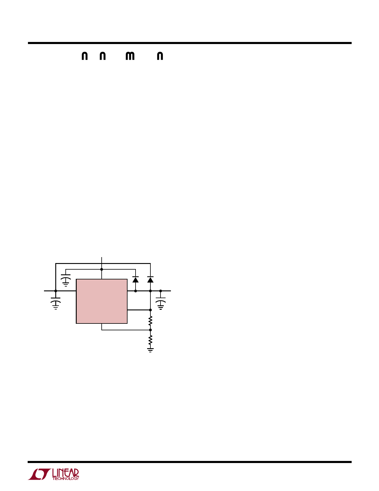
VCONTROL
+
VPOWER +
CONTROL
POWER
OUTPUT
LT1581
SENSE
ADJ
D1* D2*
+
VOUT
R1
*OPTIONAL DIODES: 1N4002
R2
1581 F06
Figure 6. Optional Clamp Diodes Protect Against
Input Crowbar Circuits
If the LT1581 is connected as a single supply device with
the control and power input pins shorted together, the
internal diode between the output and the power input pins
will protect the control input pin.
Like any other regulator exceeding the maximum input-to-
output differential can cause the internal transistors to
break down and none of the internal protection circuitry is
then functional.
Thermal Considerations
The LT1581 has internal current and thermal limiting
designed to protect the device under overload conditions.
For continuous normal load conditions maximum junction
temperature ratings must not be exceeded. It is important
to give careful consideration to all sources of thermal
resistance from junction to ambient. This includes junc-
tion-to-case, case-to-heat sink interface and heat sink
resistance itself. Thermal resistance specifications are
given in the electrical characteristics for both the Control
section and the Power section of the device. The thermal
resistance of the Control section is given as 0.65°C/ W and
junction temperature of the Control section is allowed to
run at up to 125°C. The thermal resistance of the Power
section is given as 2.5°C/W and the junction temperature
of the Power section is allowed to run at up to 150°C. The
difference in thermal resistances between Control and
Power sections is due to thermal gradients between the
power transistor and the control circuitry.
Virtually all of the power dissipated by the device is
dissipated in the power transistor. The temperature rise in
the power transistor will be greater than the temperature
rise in the Control section so the effective thermal resis-
tance, temperature rise per watt dissipated, will be lower
in the Control section. At power levels below 12W the
temperature gradient will be less than 25°C and the
maximum ambient temperature will be determined by the
junction temperature of the Control section. This is due to
the lower maximum junction temperature in the Control
section. At power levels greater than 12W the temperature
gradient will be greater than 25°C and the maximum
ambient temperature will be determined by the Power
section. For both cases the junction temperature is deter-
mined by the total power dissipated in the device. For most
low dropout applications the power dissipation will be less
than 12W.
The power in the device is made up of two main compo-
nents: the power in the output transistor and the power in
the drive circuit. The additional power in the control circuit
is negligible.
The power in the drive circuit will be equal to:
PDRIVE = (VCONTROL – VOUT)(ICONTROL)
9
Share Link: 