TH8060JDF データシートの表示(PDF) - Melexis Microelectronic Systems
部品番号
コンポーネント説明
メーカー
TH8060JDF Datasheet PDF : 16 Pages
| |||
TH8060
LIN Bus Transceiver with integrated Voltage Regulator
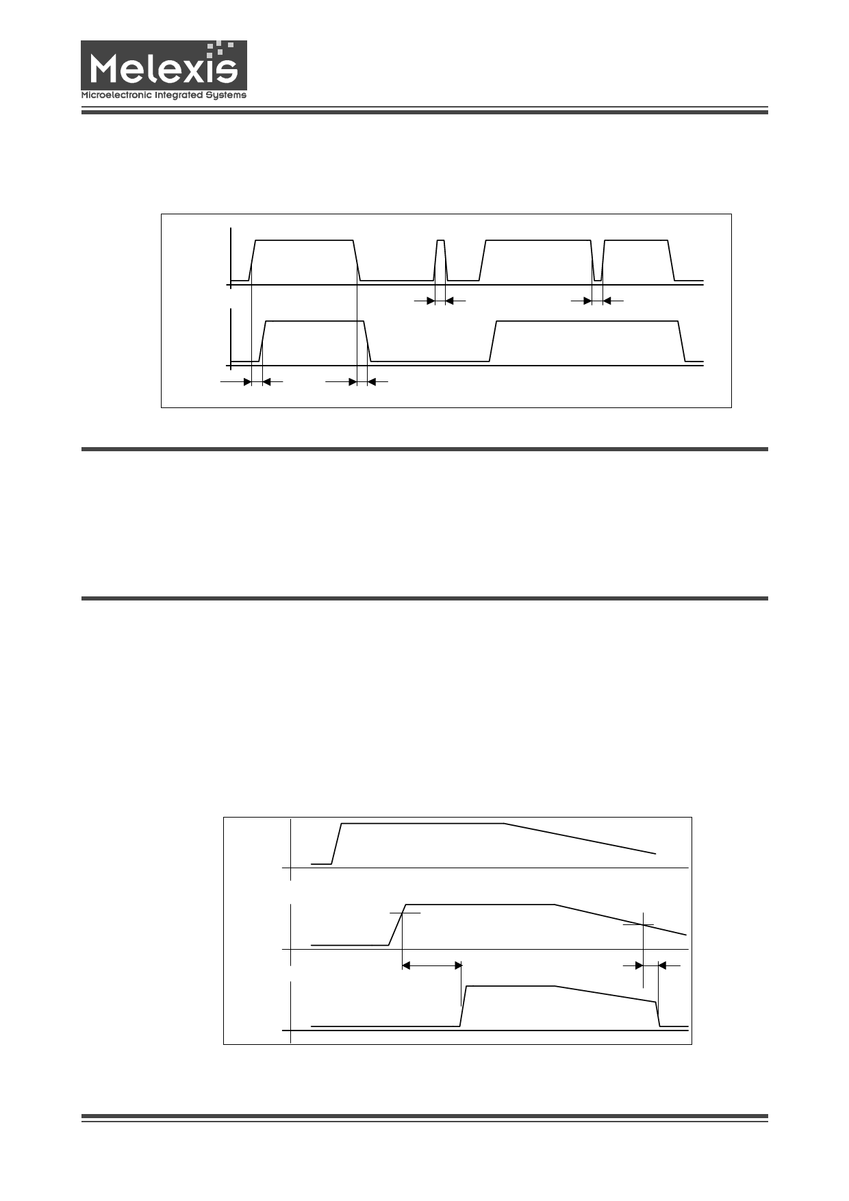
Receive Mode
The data at the pin BUS will be transferred to the pin
RxD. Short spikes on the bus signal are suppressed by
the implemented debouncing circuit.
BUS
RxD
tdebH
t < tdebH
t < tdebL
tdebL
Figure 4 - Block Diagram LIN Bus Transceiver
Linear Regulator and Controlling Functions
Regulator
The TH8060 has an integrated linear regulator with an
output voltage of 5V ±2% and an output current of
≤100mA. The regulator is switched on or off with a signal
on the EN pin or wake up with a BUS signal.
Initialization
The initialization is started if the power supply is switched
on, or after the temperature limitation has switched off
the regulator or in case of BUS traffic (wake up).
If the VCC voltage level is higher than VRESEIN, the reset
time tRES is started. This reset time is determined by the
voltage level on the VTR pin (see table VTR Program-
ming). After tRES a rising edge on the RESET output is
generated (see figure 10 - Initialization).
The regulator is active and can only switched off with a
falling edge on EN. The regulator remain with EN=high in
active mode and therefore also the VCC voltage is active.
The input EN has an internal pull down resistor. If
EN=high, the internal pull down current is switched off to
minimize the quiescent current.
VS
VCC
RESET
VRESEIN
tRes
VRES1/2
trr
Datasheet Rev 1.1 March 2001
Figure 5 - Initialization
Page 4
www.melexis.com
Share Link: 