STK551U362AGEVB データシートの表示(PDF) - ON Semiconductor
部品番号
コンポーネント説明
メーカー
STK551U362AGEVB Datasheet PDF : 16 Pages
| |||
Ordering number : ENA2210A
STK551U362A-E
Thick-Film Hybrid IC
Inverter Power H-IC
for 3-phase Motor Drive
http://onsemi.com
Overview
This “Inverter Power H-IC” is highly integrated device containing all High Voltage (HV) control from HV-DC to
3-phase outputs in a single SIP module (Single-In line Package). Output stage uses IGBT/FRD technology and
implements Under Voltage Protection (UVP) and Over Current Protection (OCP) with a Fault Detection output flag.
Internal Boost diodes are provided for high side gate boost drive.
Function
Single control power supply due to Internal bootstrap circuit for high side pre-driver circuit
All control input and status output are at low voltage levels directly compatible with microcontrollers
Built-in dead time for shoot-thru protection
Externally accessible embedded thermistor for substrate temperature measurement
The level of the over-current protection current is adjustable with the external resistor, “RSD”
Certification
UL1557 (File Number : E339285).
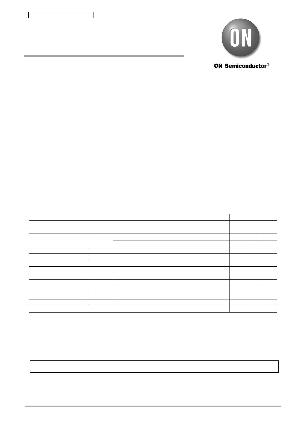
Specifications
Absolute Maximum Ratings at Tc = 25C
Parameter
Symbol
Conditions
Supply voltage
VCC
V+ to V-, surge < 500V
Collector-emitter voltage
VCE
V+ to U,V,W or U,V,W to V-
Output current
V+, V-, U,V,W terminal current
Io
V+, V-, U,V,W terminal current at Tc = 100C
Output peak current
Iop
V+, V-, U,V,W terminal current for a Pulse width of 1ms.
Pre-driver voltage
VD1,2,3,4
VB1 to U, VB2 to V, VB3 to W, VDD to VSS
Input signal voltage
VIN
HIN1, 2, 3, LIN1, 2, 3
FAULT terminal voltage
VFAULT
FAULT terminal
Maximum power dissipation
Pd
IGBT per channel
Junction temperature
Tj
IGBT,FRD
Storage temperature
Tstg
Operating case temperature
Tc
H-IC case temperature
Tightening torque
Case mounting screws
Withstand voltage
Vis
50Hz sine wave AC 1 minute
Ratings
*1
450
600
±10
±5
±20
*2
20
0.3 to VDD
0.3 to VDD
30
150
40 to +125
40 to +100
*3
1.0
*4
2000
Unit
V
V
A
A
A
V
V
V
W
C
C
C
Nm
VRMS
Reference voltage is “VSS” terminal voltage unless otherwise specified.
*1: Surge voltage developed by the switching operation due to the wiring inductance between + and U-(V-, W-) terminal.
*2: Terminal voltage: VD1=VB1-U, VD2=VB2-V, VD3=VB3-W, VD4=VDD-VSS
*3: Flatness of the heat-sink should be 0.15mm and below.
*4: Test conditions : AC2500V, 1 second.
Stresses exceeding Maximum Ratings may damage the device. Maximum Ratings are stress ratings only. Functional operation above the Recommended Operating
Conditions is not implied. Extended exposure to stresses above the Recommended Operating Conditions may affect device reliability.
ORDERING INFORMATION
See detailed ordering and shipping information on page 15 of this data sheet.
Semiconductor Components Industries, LLC, 2013
December, 2013 Ver.131206YK
D1813HK 018-13-0060/72913HK No.A2210-1/15
Share Link: 