TS3310DB データシートの表示(PDF) - Unspecified
部品番号
コンポーネント説明
メーカー
TS3310DB Datasheet PDF : 4 Pages
| |||
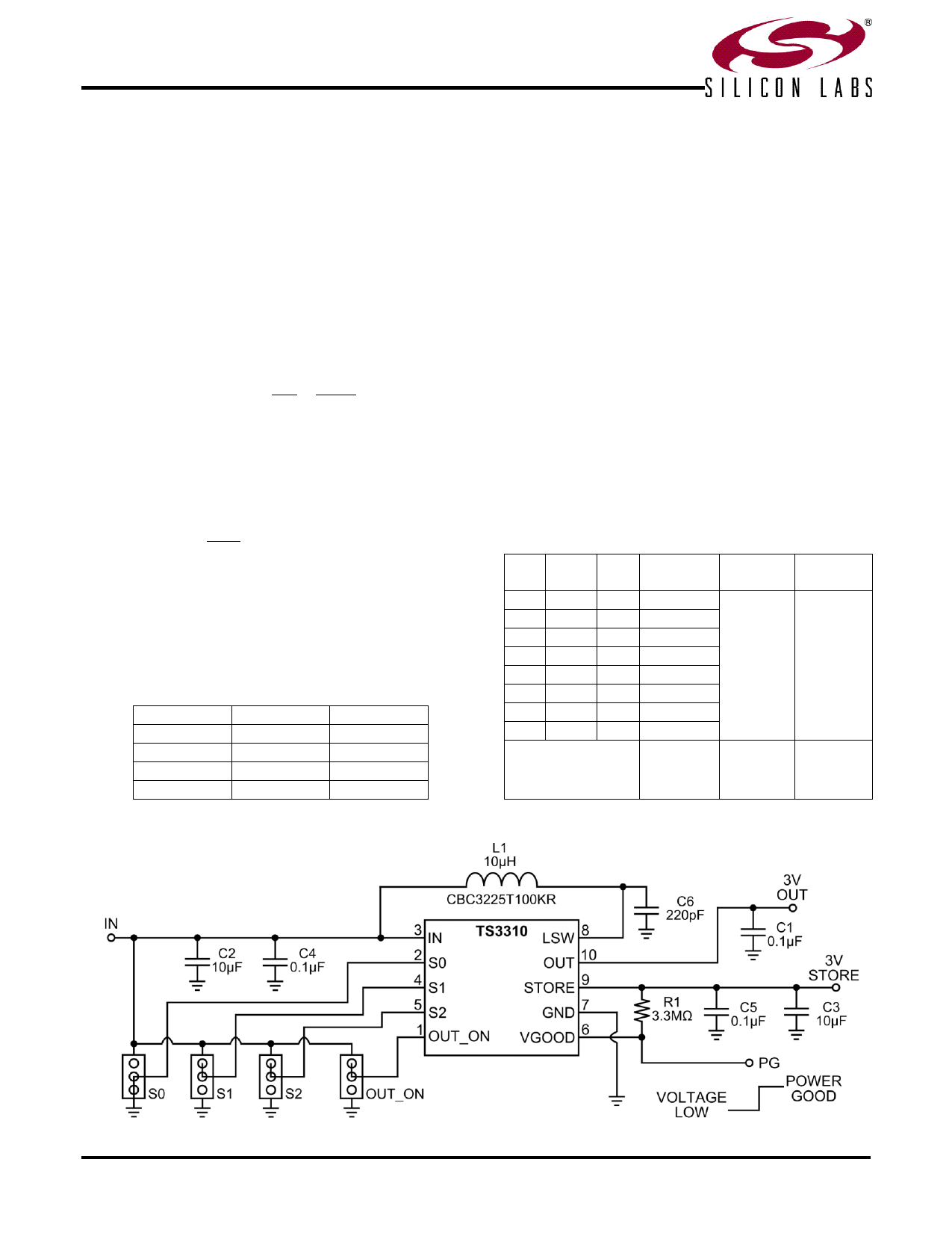
TS3310 Demo Board
DESCRIPTION
The TS3310DB is configured for 10µH inductor
operation and includes a 220pF CLSW capacitor which
is connected from the LSW pin to PCB ground,
otherwise labeled C6 on the demo board.
The maximum available output current for the
TS3310 is a function of the inductor value and the
average input current. The average input current will
vary according to the load. When the output current is
at its maximum, the averaged input current is at a
maximum. The maximum averaged input current is
defined by Equation 1.
IIN(AVG,MAX)=
Ipk
2
=
1µs∙V
L
Equation 1. Maximum Average Input Current
Calculation
The expected maximum STORE output current is
defined by Equation 2.
ISTORE(MAX)=
VIN
VOUT
× IIN(AVG,MAX) × Efficiency
Equation 2. Expected Maximum STORE Output
Current Calculation
Table 1 lists some example inductor values and the
corresponding expected maximum output load
current available for the TS3310, assuming an 85%
efficiency.
L
10µH
22µH
33µH
100µH
CLSW
220pF
100pF
---
---
ISTORE(MAX)
35mA
15mA
10mA
3mA
Table 1. Expected Maximum STORE Output
Current per Inductor Value
The TS3310 demo board is configured for 3V output
by default. With a 1.2V input voltage, the TS3310DB
which is configured for 10µH operation can supply a
maximum STORE output current of approximately
35mA.
The TS3310 demo board provides test points to
monitor the output voltage STORE and OUT. The
power good pin, VGOOD, is pulled to the STORE
output by a 3.3MΩ pull-up resistor R1 and can be
monitored via test point PG. To enable or disable the
OUT output voltage, a jumper for the OUT_ON pin is
available. The STORE and OUT output voltage can
be set via jumpers S2, S1, and S0.
Table 2 displays the S2, S1, and S0 combinations
along with the corresponding output voltage. For 5V
output operation, a minimum input voltage of 2V is
required. The TS3310 demo board circuit in its default
configuration, with a 3V output voltage, is displayed in
Figure 3.
S2 S1 S0
000
001
010
011
100
101
110
111
Same as Above
STORE
(V)
1.8
2.5
3.3
5
2.1
2.85
3
4.1
OUT_ON
OUT
(V)
HIGH
Equal to
STORE
(V)
Same as
Above
LOW
0V
Table 2. STORE and OUT Voltage Settings
TS3310-EVB Rev. 1.0
Figure 3. TS3310DB Circuit Schematic
Page 2
Share Link: 