NCP4355C データシートの表示(PDF) - ON Semiconductor
部品番号
コンポーネント説明
メーカー
NCP4355C Datasheet PDF : 17 Pages
| |||
NCP4355
APPLICATION INFORMATION
Typical application circuits for NCP4355x are shown in
Figure 24, Figure 25 and Figure 26. Each IC version contains
different features. Please see Device options table or Block
diagrams for detail information. NCP4355A does not have
a VMIN pin for setting the minimum voltage level, therefore
it needs a special circuit shown in Figure 24 in the dashed
box. This is needed for correct detection of load connection
in OFF mode. The same circuit can be used for other versions
when high speed detection of load connection is needed.
Supply Voltage
The IC is supplied through VCC pin. Supply voltage
should be taken from output voltage in range from 4.5 V up
to 36 V. Power supply voltage should be separated from
output voltage by a diode D3 and some energy should be
stored in a VCC cap C6. Cap should be high enough to keep
enough energy for ONOFF optocoupler and NCP4355x
before primary controller is started. Time constant of the
VCC cap C6 and the IC supply current should be smaller
than time constant of power supply output filter and
maximum output current in OFF mode. VCC pin should also
be decoupled by 100 nF decoupling cap C5.
Voltage Regulation Path
The output voltage is detected on the VSNS pin by the R4,
R5 and R6 voltage divider. This voltage is compared with
the internal precise voltage reference. The voltage
difference is amplified by gmV of the transconductance
amplifier. The amplifier output current is connected to the
FBC pin. The compensation network is also connected to
this pin to provide frequency compensation for the voltage
regulation path. This FBC pin drives an optocoupler that
provides regulation of primary side. The optocoupler is
supplied via direct connection to VOUT line through
resistor R1.
Regulation information is transferred through the
optocoupler to the primary side controller where its FB pin
is usually pulled down to reduce energy transferred to
secondary output.
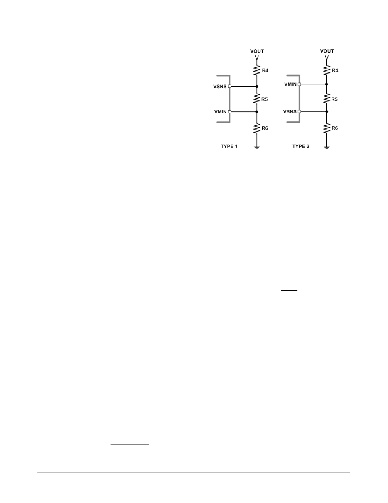
The VSNS voltage divider is shared with VMIN voltage
divider. The shared voltage divider can be connected in two
ways as shown in Figure 23. The divider type is selected
based on the ratio between VMIN and VOUT. When the
condition of Equation 1 is true, divider type 1 should be used.
VMIN
u
VOUT VREFM
VREF
(eq. 1)
Output voltage for divider type 1 can be computed by
Equation 2
VOUT
+
VREF
R4 ) R5 ) R6
R5 ) R6
(eq. 2)
and for type 2 by Equation 3.
VOUT
+
VREF
R4
)
R5
R6
)
R6
(eq. 3)
Figure 23. Shared Dividers Type
Current Regulation Path (A and C versions only)
The output current is sensed by the shunt resistor R11 in
series with the load. Voltage drop on R11 is compared with
internal precise voltage reference VREFC at ISNS transcon−
ductance amplifier input.
Voltage difference is amplified by gmC to output current
of amplifier, connected to FBC pin. Compensation network
is connected between this pin and ISNS input to provide
frequency compensation for current regulation path.
Resistor R12 separates compensation network from sense
resistor. Compensation network works into low impedance
without this resistor that significantly decreases
compensation network impact.
Current regulation point is set to current given by
Equation 4.
IOUTLIM
+
VREFC
R11
(eq. 4)
OFF Mode Detection
OFF mode operation is advantageous for ultra low or zero
output current condition. The very long off time and the ultra
low power mode of the whole regulation system greatly
reduces the overall consumption.
The output voltage is varying between nominal and
minimal in OFF mode. When output voltage decreases
below set (except NCP4355A) minimum level, primary
controller is switch on until output capacitor C1 is charged
again to the nominal voltage.
The OFF mode detection is based on comparison of output
voltage and voltage loaded with fixed resistances (D2, C2,
R7 and R8). Figure 27 shows detection waveforms. When
output voltage is loaded with very low current, primary
controller goes into skip mode (primary controller stops
switching for some time). While output capacitor C1 is
discharged very slowly (no load condition), a fixed load R7
and R8 discharges the capacitor C2 faster than load current
discharges output voltage on C1.
Once OFFDET pin voltage is lower than VOFFDETTH (this
threshold is derived from VCC that is very close to VOUT),
http://onsemi.com
10
Share Link: 