2SJ407(2004) データシートの表示(PDF) - Toshiba
部品番号
コンポーネント説明
メーカー
2SJ407 Datasheet PDF : 6 Pages
| |||
2SJ407
TOSHIBA Field Effect Transistor Silicon P Channel MOS Type (π−MOSV)
2SJ407
Chopper Regulator, DC−DC Converter and Motor Drive
Applications
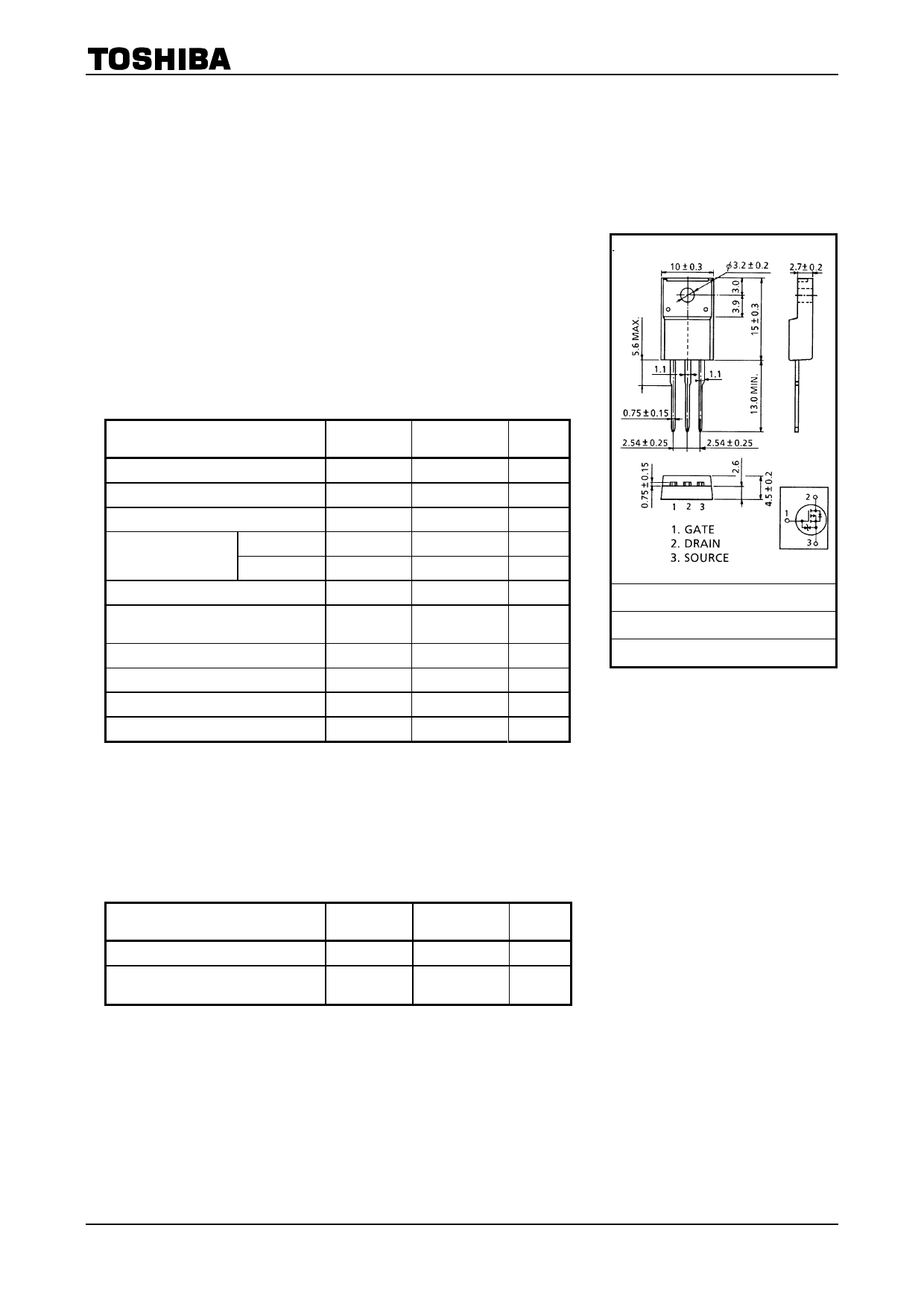
Unit: mm
Low drain−source ON resistance : RDS (ON) = 0.8 Ω (typ.)
High forward transfer admittance : |Yfs| = 4.0 S (typ.)
Low leakage current : IDSS = −100 µA (max) (VDS = −200 V)
Enhancement mode : Vth = −1.5~−3.5 V (VDS = −10 V, ID = −1 mA)
Maximum Ratings (Ta = 25°C)
Characteristics
Symbol
Rating
Unit
Drain−source voltage
Drain−gate voltage (RGS = 20 kΩ)
Gate−source voltage
Drain current
DC (Note 1)
Pulse(Note 1)
Drain power dissipation (Tc = 25°C)
Single pulse avalanche energy
(Note 2)
Avalanche current
Repetitive avalenche energy (Note 3)
Channel temperature
Storage temperature range
VDSS
VDGR
VGSS
ID
IDP
PD
EAS
IAR
EAR
Tch
Tstg
−200
V
−200
V
±20
V
−5
A
−20
A
30
W
195
mJ
−5
A
3.0
mJ
150
°C
−55~150
°C
JEDEC
―
JEITA
SC-67
TOSHIBA
2-10R1B
Weight: 1.9 g (typ.)
Thermal Characteristics
Characteristics
Symbol
Max
Unit
Thermal resistance, channel to case
Thermal resistance, channel to
ambient
Rth (ch−c)
Rth (ch−a)
4.16
°C / W
62.5
°C / W
Note 1: Ensure that the channel temperature does not exceed 150°C.
Note 2: VDD = −50 V, Tch = 25°C (initial), L = 12.6 mH, RG = 25 Ω, IAR = −5 A
Note 3: Repetitive rating: pulse width limited by maximum channel temperature
This transistor is an electrostatic-sensitive device.
Please handle with caution.
1
2004-07-06
Share Link: 