SI4704-D50 データシートの表示(PDF) - Silicon Laboratories
部品番号
コンポーネント説明
メーカー
SI4704-D50 Datasheet PDF : 34 Pages
| |||
Si4704/05-D50
1. Electrical Specifications
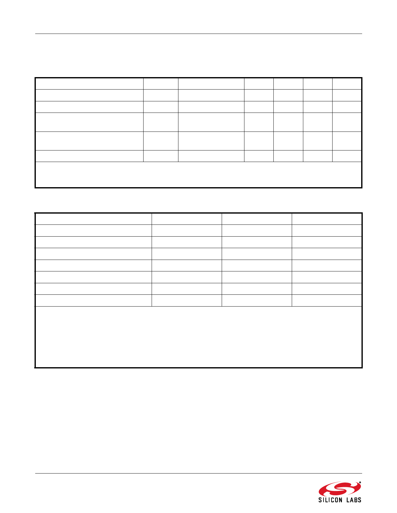
Table 1. Recommended Operating Conditions*
Parameter
Symbol Test Condition
Min
Typ
Max
Unit
Analog Supply Voltage
Digital and Interface Supply Voltage
Analog Power Supply Powerup Rise
Time
VA
VD
VARISE
2.7
—
5.5
V
1.62
—
3.6
V
10
—
—
µs
Digital Power Supply Powerup Rise VDRISE
Time
10
—
—
µs
Ambient Temperature
TA
–20
25
85
C
*Note: All minimum and maximum specifications are guaranteed and apply across the recommended operating conditions.
Typical values apply at VA = 3.3 V and 25 C unless otherwise stated. Parameters are tested in production unless
otherwise stated.
Table 2. Absolute Maximum Ratings1,2
Parameter
Symbol
Value
Unit
Analog Supply Voltage
VA
–0.5 to 5.8
V
Digital and Interface Supply Voltage
Input Current3
Input Voltage3
VD
–0.5 to 3.9
V
IIN
10
mA
VIN
–0.3 to (VIO + 0.3)
V
Operating Temperature
TOP
–40 to 95
C
Storage Temperature
RF Input Level4
TSTG
–55 to 150
C
0.4
VpK
Notes:
1. Permanent device damage may occur if the above Absolute Maximum Ratings are exceeded. Functional operation
should be restricted to the conditions as specified in the operational sections of this data sheet. Exposure beyond
recommended operating conditions for extended periods may affect device reliability.
2. The Si4704/05 devices are high-performance RF integrated circuits with certain pins having an ESD rating of < 2 kV
HBM. Handling and assembly of these devices should only be done at ESD-protected workstations.
3. For input pins DFS, SCLK, SEN, SDIO, RST, RCLK, GPO1, GPO2, GPO3, and DCLK.
4. At RF input pins FMI and LPI.
4
Rev. 1.0
Share Link: 