HV9963NG-G データシートの表示(PDF) - Supertex Inc
部品番号
コンポーネント説明
メーカー
HV9963NG-G Datasheet PDF : 12 Pages
| |||
HV9963
AVDD
-
ISC
+
GATE
Q2
GND
RT
CS
CSC
AVDD
RCS
-
ISC
+
GATE
Q2
GND
GATE
RT
CS CSC
Q1
CDRAIN
RCS
+
VDRAIN
-
- VLP +
LP
ILP
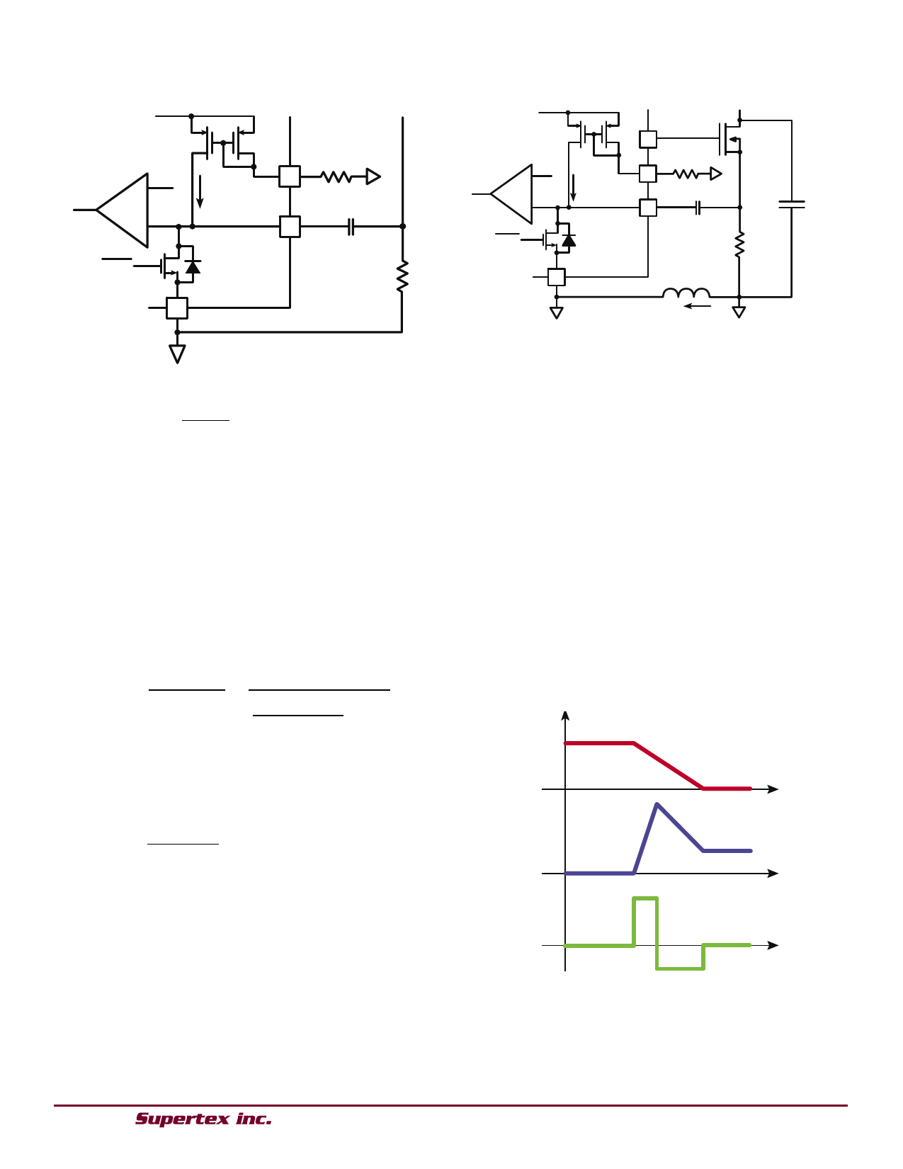
Figure 2: Slope Compensation circuit with parasitics
Figure 1: Slope Compensation circuit
ISC =
2µA
•
fS
100kHz
This current flows into the capacitor and produces a ramp
voltage across the capacitor. The voltage at the CS pin is
then the sum of the voltage across the capacitor and the
voltage across the current sense resistor, with the voltage
across the capacitor providing the required slope compen-
sation. When the GATE turns off, an internal pull down FET
discharges the capacitor.
Assuming a down slope of DS (A/μs) for the inductor current,
the current sense resistor can be computed as:
RCS =
AVDD - 0.9V
12
•
1
DS • 106 • 0.93
2 • fS
+ ISAT
When the FET Q1 is off, the internal discharge to FET Q2
is turned on and capacitor CSC is discharged. Also, CDRAIN
is charged to the output voltage VO. When the FET Q1 is
turned on, the drain node of the FET is pulled to ground (Q2
is turned off just prior to Q1 being turned on). This causes
the drain capacitance to discharge through the FET Q1,
causing a current spike as shown in Figure 3. This current
spike causes a voltage to develop across the parasitic in-
ductance. As long as the current is increasing through the in-
ductance, the voltage developed across the inductor is suc-
cessfully blocked by the body diode of Q2. However, during
the falling edge of the current spike, the voltage across the
inductor causes the body diode to become forward biased.
This conduction path through the body diode of Q2 causes
pre-charge of CSC. The pre-charge voltage can be fairly high
since the current’s rate of fall is very large.
The slope compensation capacitor is chosen to provide the
required amount of slope compensation required to maintain
stability.
CSC
=
ISC
DS/2 •
RCS
VDRAIN
ILP
Note: Sometimes, excessive stray inductance in the current
sense path might cause the slope compensation circuit to
mis-trigger. The following section describes the cause of the
VLP
problem and the solution.
Figure 2 shows the detailed slope compensation circuit with
a parasitic inductance LP between the ground of the boost
converter and the ground of the HV9963. Also shown is the
drain capacitance of the boost FET Q1 (which is the total
capacitance at the drain node).
Figure 3: Waveforms during turn-on
For example, a typical current spike usually lasts about
100ns. Assuming a 3A peak current (this value is usually the
saturation current of the FET which can be much higher) and
● 1235 Bordeaux Drive, Sunnyvale, CA 94089 ● Tel: 408-222-8888 ● www.supertex.com
7
Share Link: 