MC33264D-2.8 データシートの表示(PDF) - Motorola => Freescale
部品番号
コンポーネント説明
メーカー
MC33264D-2.8 Datasheet PDF : 8 Pages
| |||
MC33264
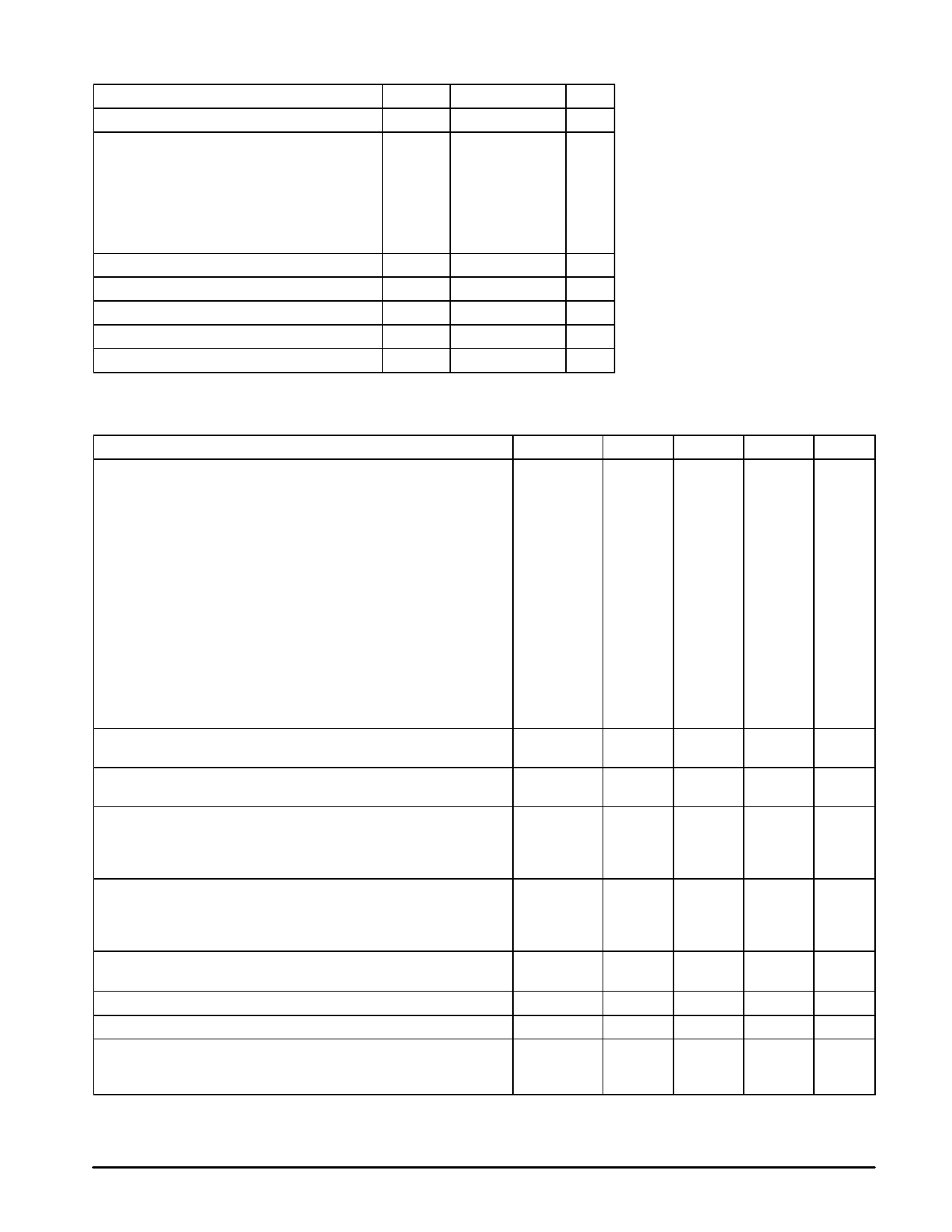
MAXIMUM RATINGS (TC = 25°C, unless otherwise noted.)
Rating
ÁÁÁÁÁÁÁÁÁÁÁÁÁÁÁÁÁÁÁÁÁÁÁ Input Voltage
ÁÁÁÁÁÁÁÁÁÁÁÁÁÁÁÁÁÁÁÁÁÁÁ Power Dissipation and Thermal Characteristics
ÁÁÁÁÁÁÁÁÁÁÁÁÁÁÁÁÁÁÁÁÁÁÁ Maximum Power Dissipation
Symbol
Value
Unit
VCC
13
Vdc
PD
Internally Limited W
Case 751 (SO–8) D Suffix
Thermal Resistance, Junction–to–Ambient
RθJA
180
°C/W
Thermal Resistance, Junction–to–Case
RθJC
45
°C/W
Case 846A (Micro–8) DM Suffix
Thermal Resistance, Junction–to–Ambient
ÁÁÁÁÁÁÁÁÁÁÁÁÁÁÁÁÁÁÁÁÁÁÁ Output Current
ÁÁÁÁÁÁÁÁÁÁÁÁÁÁÁÁÁÁÁÁÁÁÁ Maximum Adjustable Output Voltage
ÁÁÁÁÁÁÁÁÁÁÁÁÁÁÁÁÁÁÁÁÁÁÁ Operating Junction Temperature
ÁÁÁÁÁÁÁÁÁÁÁÁÁÁÁÁÁÁÁÁÁÁÁ Operating Ambient Temperature
ÁÁÁÁÁÁÁÁÁÁÁÁÁÁÁÁÁÁÁÁÁÁÁÁÁÁÁÁÁÁÁÁÁÁÁÁÁÁÁÁÁÁÁÁÁÁ Storage Temperature Range
RθJA
IO
VO
TJ
TA
Tstg
240
100
1.15 x Vnom
125
–40 to +85
–65 to +150
°C/W
mA
Vdc
°C
°C
°C
NOTE: ESD data available upon request.
ELECTRICAL CHARACTERISTICS (Vin = 6.0 V, IO = 10 mA, CO = 1.0 µF, TJ = 25°C (Note 1), unless otherwise noted.)
Characteristic
ÁÁÁÁÁÁÁÁÁÁÁÁÁÁÁÁÁÁÁÁÁÁÁÁÁÁÁÁÁÁÁÁÁÁ Output Voltage (IO = 0 mA)
ÁÁÁÁÁÁÁÁÁÁÁÁÁÁÁÁÁÁÁÁÁÁÁÁÁÁÁÁÁÁÁÁÁÁ 2.8 Suffix (VCC = 3.8 V)
Symbol
Min
Typ
Max
Unit
VO
V
2.74
2.8
2.86
3.0 Suffix (VCC = 4.0 V)
2.96
3.0
3.04
3.3 Suffix (VCC = 4.3 V)
3.23
3.3
3.37
3.8 Suffix (VCC = 4.8 V)
3.72
3.8
3.88
4.0 Suffix (VCC = 5.0 V)
3.92
4.0
4.08
4.75 Suffix (VCC = 5.75 V)
4.66
4.75
4.85
5.0 Suffix (VCC = 6.0 V)
4.9
5.0
5.1
Vin = (VO + 1.0) V to 12 V, IO < 60 mA,TA= –40° to +85°C
2.8 Suffix
2.7
–
2.9
3.0 Suffix
2.9
–
3.1
3.3 Suffix
3.18
–
3.42
3.8 Suffix
3.67
–
3.93
4.0 Suffix
3.86
–
4.14
4.75 Suffix
4.58
–
4.92
5.0 Suffix
ÁÁÁÁÁÁÁÁÁÁÁÁÁÁÁÁÁÁÁÁÁÁÁÁÁÁÁÁÁÁÁÁÁÁ Line Regulation (Vin = [VO + 1.0] V to 12 V, IO = 60 mA)
All Suffixes
ÁÁÁÁÁÁÁÁÁÁÁÁÁÁÁÁÁÁÁÁÁÁÁÁÁÁÁÁÁÁÁÁÁÁÁÁÁÁÁÁÁÁÁÁÁÁÁÁÁÁÁÁÁÁÁÁÁÁÁÁÁÁÁÁÁÁÁÁ Load Regulation (Vin = [VO + 1.0], IO = 0 mA to 60 mA)
All Suffixes
ÁÁÁÁÁÁÁÁÁÁÁÁÁÁÁÁÁÁÁÁÁÁÁÁÁÁÁÁÁÁÁÁÁÁ Dropout Voltage
ÁÁÁÁÁÁÁÁÁÁÁÁÁÁÁÁÁÁÁÁÁÁÁÁÁÁÁÁÁÁÁÁÁÁ IO = 10 mA
4.83
–
5.17
Regline
–
2.0
10
mV
Regload
–
16
25
mV
VI – VO
–
mV
47
90
IO = 50 mA
IO = 60 mA
ÁÁÁÁÁÁÁÁÁÁÁÁÁÁÁÁÁÁÁÁÁÁÁÁÁÁÁÁÁÁÁÁÁÁ Quiescent Current
ÁÁÁÁÁÁÁÁÁÁÁÁÁÁÁÁÁÁÁÁÁÁÁÁÁÁÁÁÁÁÁÁÁÁ ON Mode (Vin = [VO + 1.0] V, IO = 0 mA)
–
131
200
–
147
230
IQ
µA
–
95
150
OFF Mode
ON Mode (Vin = [VO + 0.5] V, IO = 0 mA) [Note2]
ÁÁÁÁÁÁÁÁÁÁÁÁÁÁÁÁÁÁÁÁÁÁÁÁÁÁÁÁÁÁÁÁÁÁ Ripple Rejection (Vin peak–to–peak = [VO + 1.5] to [VO + 5.5]
ÁÁÁÁÁÁÁÁÁÁÁÁÁÁÁÁÁÁÁÁÁÁÁÁÁÁÁÁÁÁÁÁÁÁ V at f = 1.0 kHz)
ÁÁÁÁÁÁÁÁÁÁÁÁÁÁÁÁÁÁÁÁÁÁÁÁÁÁÁÁÁÁÁÁÁÁ Output Voltage Temperature Coefficient
ÁÁÁÁÁÁÁÁÁÁÁÁÁÁÁÁÁÁÁÁÁÁÁÁÁÁÁÁÁÁÁÁÁÁ Current Limit (Vin = [VO + 1.0], VO Shorted)
ÁÁÁÁÁÁÁÁÁÁÁÁÁÁÁÁÁÁÁÁÁÁÁÁÁÁÁÁÁÁÁÁÁÁ Output Noise Voltage (10 Hz to 100 kHz) (Note 3)
ÁÁÁÁÁÁÁÁÁÁÁÁÁÁÁÁÁÁÁÁÁÁÁÁÁÁÁÁÁÁÁÁÁÁ CL = 1.0 µF
–
TC
ILimit
Vn
–
0.3
2.0
–
540
900
55
65
–
dB
–
±120
100
150
–
110
–
ppm/°C
–
mA
µVrms
–
CL = 100 µF
–
46
–
NOTES: 1. Low duty pulse techniques are used during test to maintain junction temperature as close to ambient as possible.
2. Quiescent current is measured where the PNP pass transistor is in saturation. VCE = –0.5 V guarantees this condition.
3. Noise tests on the MC33264 are made with a 0.01 µF capacitor connected across Pins 8 and 5.
2
MOTOROLA ANALOG IC DEVICE DATA
Share Link: 