ADA4932-1 データシートの表示(PDF) - Analog Devices
部品番号
コンポーネント説明
メーカー
ADA4932-1 Datasheet PDF : 28 Pages
| |||
ABSOLUTE MAXIMUM RATINGS
Table 7.
Parameter
Supply Voltage
Power Dissipation
Input Current, +IN, −IN, PD
Storage Temperature Range
Operating Temperature Range
ADA4932-1
ADA4932-2
Lead Temperature (Soldering, 10 sec)
Junction Temperature
Rating
11 V
See Figure 4
±5 mA
−65°C to +125°C
−40°C to +105°C
−40°C to +105°C
300°C
150°C
Stresses above those listed under Absolute Maximum Ratings
may cause permanent damage to the device. This is a stress
rating only; functional operation of the device at these or any
other conditions above those indicated in the operational section of
this specification is not implied. Exposure to absolute maximum
rating conditions for extended periods may affect device
reliability.
THERMAL RESISTANCE
θJA is specified for the device (including exposed pad) soldered
to a high thermal conductivity 2s2p circuit board, as described
in EIA/JESD 51-7.
Table 8. Thermal Resistance
Package Type
ADA4932-1, 16-Lead LFCSP (Exposed Pad)
ADA4932-2, 24-Lead LFCSP (Exposed Pad)
θJA Unit
91 °C/W
65 °C/W
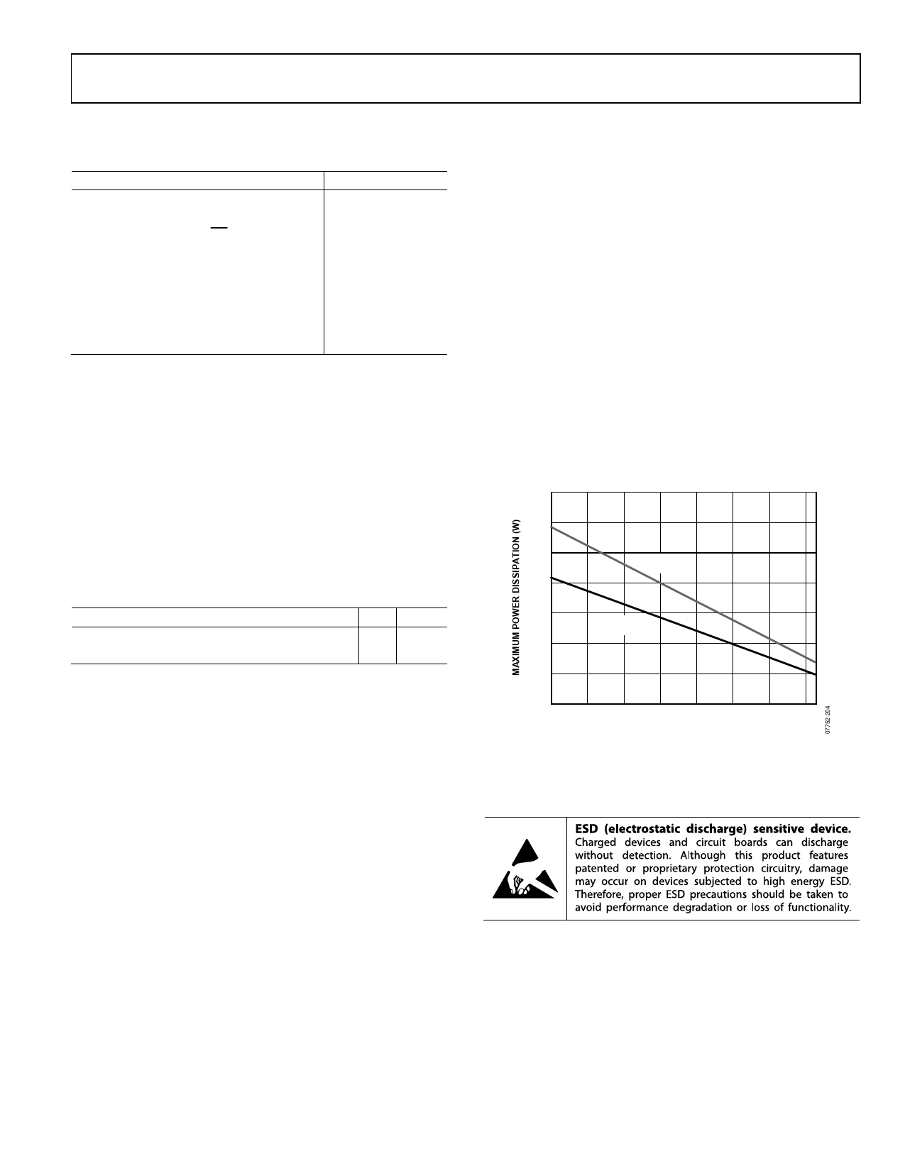
MAXIMUM POWER DISSIPATION
The maximum safe power dissipation in the ADA4932-x
package is limited by the associated rise in junction temperature
(TJ) on the die. At approximately 150°C, which is the glass
transition temperature, the plastic changes its properties. Even
temporarily exceeding this temperature limit can change the
stresses that the package exerts on the die, permanently shifting
the parametric performance of the ADA4932-x. Exceeding a
junction temperature of 150°C for an extended period can result
in changes in the silicon devices, potentially causing failure.
ADA4932-1/ADA4932-2
The power dissipated in the package (PD) is the sum of the
quiescent power dissipation and the power dissipated in the
package due to the load drive. The quiescent power is the voltage
between the supply pins (VS) times the quiescent current (IS).
The power dissipated due to the load drive depends upon the
particular application. The power due to load drive is calculated
by multiplying the load current by the associated voltage drop
across the device. RMS voltages and currents must be used in
these calculations.
Airflow increases heat dissipation, effectively reducing θJA. In
addition, more metal directly in contact with the package leads/
exposed pad from metal traces, through holes, ground, and power
planes reduces θJA.
Figure 4 shows the maximum safe power dissipation in the
package vs. the ambient temperature for the single 16-lead
LFCSP (91°C/W) and the dual 24-lead LFCSP (65°C/W) on a
JEDEC standard 4-layer board with the exposed pad soldered to
a PCB pad that is connected to a solid plane.
3.5
3.0
2.5
ADA4932-2
2.0
1.5
ADA4932-1
1.0
0.5
0
–40
–20
0
20
40
60
80
100
AMBIENT TEMPERATURE (°C)
Figure 4. Maximum Power Dissipation vs. Ambient Temperature for
a 4-Layer Board
ESD CAUTION
Rev. A | Page 7 of 28
Share Link: 