ADA4932-1 データシートの表示(PDF) - Analog Devices
部品番号
コンポーネント説明
メーカー
ADA4932-1 Datasheet PDF : 28 Pages
| |||
ADA4932-1/ADA4932-2
PIN CONFIGURATIONS AND FUNCTION DESCRIPTIONS
–FB 1
+IN 2
–IN 3
+FB 4
PIN 1
INDICATOR
ADA4932-1
TOP VIEW
(Not to Scale)
12 PD
11 –OUT
10 +OUT
9 VOCM
–IN1 1
+FB1 2
+VS1 3
+VS1 4
–FB2 5
+IN2 6
PIN 1
INDICATOR
ADA4932-2
TOP VIEW
(Not to Scale)
18 +OUT1
17 VOCM1
16 –VS2
15 –VS2
14 PD2
13 –OUT2
NOTES
1. SOLDER EXPOSED PADDLE ON BACK OF PACKAGE
TO GROUND PLANE OR TO A POWER PLANE.
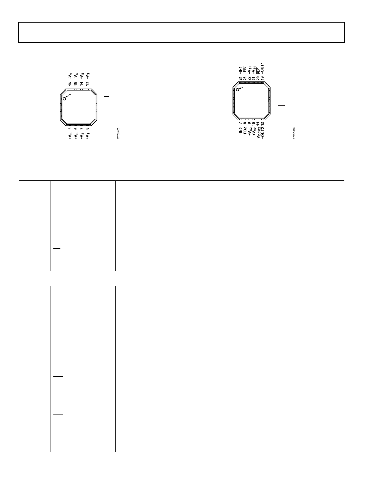
Figure 5. ADA4932-1 Pin Configuration
NOTES
1. SOLDER EXPOSED PADDLE ON BACK OF PACKAGE
TO GROUND PLANE OR TO A POWER PLANE.
Figure 6. ADA4932-2 Pin Configuration
Table 9. ADA4932-1 Pin Function Descriptions
Pin No. Mnemonic
Description
1
−FB
Negative Output for Feedback Component Connection.
2
+IN
Positive Input Summing Node.
3
−IN
Negative Input Summing Node.
4
+FB
Positive Output for Feedback Component Connection.
5 to 8
9
10
+VS
VOCM
+OUT
Positive Supply Voltage.
Output Common-Mode Voltage.
Positive Output for Load Connection.
11
−OUT
Negative Output for Load Connection.
12
PD
Power-Down Pin.
13 to 16 −VS
17 (EPAD) Exposed Paddle (EPAD)
Negative Supply Voltage.
Solder the exposed paddle on the back of the package to a ground plane or to a power plane.
Table 10. ADA4932-2 Pin Function Descriptions
Pin No. Mnemonic
Description
1
−IN1
Negative Input Summing Node 1.
2
+FB1
Positive Output Feedback 1.
3, 4
+VS1
Positive Supply Voltage 1.
5
−FB2
Negative Output Feedback 2.
6
+IN2
Positive Input Summing Node 2.
7
−IN2
Negative Input Summing Node 2.
8
+FB2
Positive Output Feedback 2.
9, 10
+VS2
Positive Supply Voltage 2.
11
VOCM2
Output Common-Mode Voltage 2.
12
+OUT2
Positive Output 2.
13
−OUT2
Negative Output 2.
14
PD2
Power-Down Pin 2.
15, 16
−VS2
Negative Supply Voltage 2.
17
VOCM1
Output Common-Mode Voltage 1.
18
+OUT1
Positive Output 1.
19
−OUT1
Negative Output 1.
20
PD1
Power-Down Pin 1.
21, 22
−VS1
Negative Supply Voltage 1.
23
−FB1
Negative Output Feedback 1.
24
+IN1
Positive Input Summing Node 1.
25 (EPAD) Exposed Paddle (EPAD) Solder the exposed paddle on the back of the package to a ground plane or to a power plane.
Rev. A | Page 8 of 28
Share Link: 