C8051F120DK データシートの表示(PDF) - Silicon Laboratories
部品番号
コンポーネント説明
メーカー
C8051F120DK Datasheet PDF : 13 Pages
| |||
C8051F12x-DK
6.6. PORT I/O Connectors (J12 - J19)
In addition to all port I/O signals being routed to the 96-pin expansion connector, each of the eight parallel ports of
the C8051F120 has its own 10-pin header connector. Each connector provides a pin for the corresponding port
pins 0-7, +3.3 VDC and digital ground. Table 5 defines the pins for the port connectors. The same pin-out order is
used for all of the port connectors.
Table 5. J12- J19 Port Connector Pin Descriptions
Pin #
1
2
3
4
5
6
7
8
9
10
Description
Pn.0
Pn.1
Pn.2
Pn.3
Pn.4
Pn.5
Pn.6
Pn.7
+3 VD (+3.3 VDC)
GND (Ground)
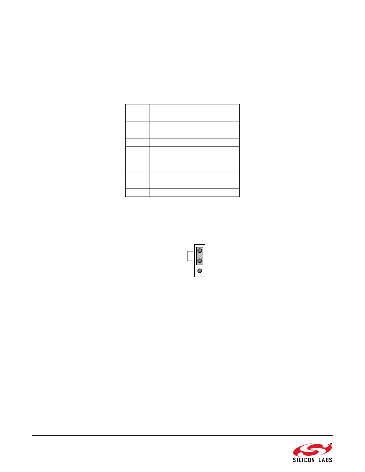
6.7. VDD Monitor Disable (J23)
The VDD Monitor of the C8051F120 may be disabled by moving the shorting block on J23 from pins 1-2 to pins 2-
3, as shown in Figure 3.
1
MONEN
2
3
Figure 3. VDD Monitor Hardware Setup
6.8. VREF Connector (J22)
The VREF connector (J22) can be used to connect the VREF (Voltage Reference) output of the C8051F120 to any
(or all) of its voltage reference inputs. Install shorting blocks on J22 in the following manner:
1–2 to connect VREF to VREFD
3–4 to connect VREF to VREF0
5–6 to connect VREF to VREF1
8
Rev. 0.7
Share Link: 