BD2802 データシートの表示(PDF) - ROHM Semiconductor
部品番号
コンポーネント説明
メーカー
BD2802 Datasheet PDF : 28 Pages
| |||
BD2802GU
Technical Note
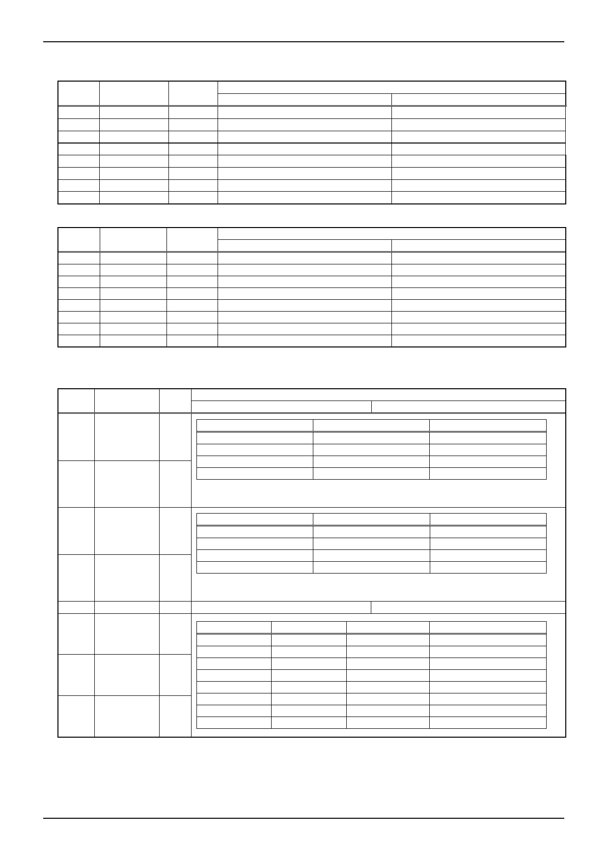
●Register Description
Adress 00h <Soft Reset>
BIT
Name
Initial
D7
-
-
D6
-
-
D5
CLKMD
0
D4
CLKEN
0
D3
-
-
D2
-
-
D1
-
-
D0
SFTRST
0
0
-
-
Clock Input mode
Clock input and output invalid
-
-
-
Reset Release
Function
1
-
-
Clock Output mode
Clock input and output Effective
-
-
-
Reset
Adress 01h <RGB LED control >
BIT
Name
Init
Function
0
D7
-
-
-
D6
RGB2MEL
0
RGB2 external control invalid
D5
RGB2OS
0
RGB2 Stop
D4
RGB2EN
0
RGB2 Stop
D3
-
-
-
D2
RGB1MEL
0
RGB1 external control invalid
D1
RGB1OS
0
RGB1 Stop
D0
RGB1EN
0
RGB1 Stop
* RGB*OS returns to 0 automatically after 1 cycle operation.
* RGB*EN precedes to RGB*OS. In use in 1 cycle operation, there is the necessity for RGB*EN=0.
1
-
RGB2 external control valid
RGB2 1 periodic operation
RGB2 continuous operation
-
RGB1 external control valid
RGB1 1 periodic operation
RGB1 continuous operation
Adress 02h <RGB1 time>
BIT
Name
Init
D7 SFRGB1(1) 0
D6 SFRGB1(0) 0
Function
0
1
SFRGB1(1)
SFRGB1(0)
Slope Down transition
0
0
0
0
1
Wave form cycle / 16
1
0
Wave form cycle / 8
1
1
Wave form cycle / 4
It is a theoretical value on logic control, and the reaction time of the analog section is
not included."Slope time" is the time from a slope start to a slope end.
D5 SRRGB1(1) 0
D4 SRRGB1(0) 0
D3
-
-
D2
TRGB1(2)
0
D1
TRGB1(1)
0
D0
TRGB1(0)
0
SRRGB1(1)
SRRGB1(0)
Slope Up transition
0
0
0
0
1
Wave form cycle / 16
1
0
Wave form cycle / 8
1
1
Wave form cycle / 4
It is a theoretical value on logic control, and the reaction time of the analog section is not
included."Slope time" is the time from a slope start to a slope end.
-
-
TRGB1(2)
0
0
0
0
1
1
1
1
TRGB1(1)
0
0
1
1
0
0
1
1
TRGB1(0)
0
1
0
1
0
1
0
1
Wave form cycle
0.131 s
0.52 s
1.05 s
2.10 s
4.19 s
8.39 s
12.6 s
16.8 s
Setting time is counted based on the frequency of OSC. The above-mentioned value is a value at the time of Typ (1MHz).
When operating by the external clock, input frequency is a value at the time of Typ (250kHz).
*Refer to "●Use of a RGB wave setup " for the detailed function of each register of this page.
www.rohm.com
© 2011 ROHM Co., Ltd. All rights reserved.
10/27
2011.04 - Rev.A
Share Link: 