IR21091SPBF データシートの表示(PDF) - International Rectifier
部品番号
コンポーネント説明
メーカー
IR21091SPBF Datasheet PDF : 8 Pages
| |||
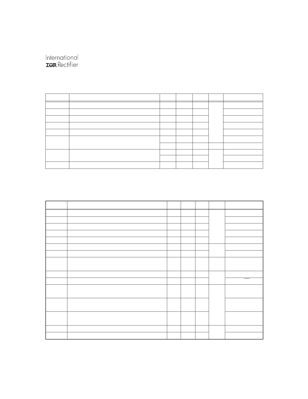
IR21091(S) & (PbF)
Dynamic Electrical Characteristics
VBIAS (VCC, VBS) = 15V, CL = 1000 pF, TA = 25°C, DT = VSS unless otherwise specified.
Symbol
ton
toff
MT
tr
tf
DT
MDT
tsd
Definition
Turn-on propagation delay
Turn-off propagation delay
Delay matching, HS & LS turn-on/off
Turn-on rise time
Turn-off fall time
Deadtime: LO turn-off to HO turn-on(DTLO-HO) &
HO turn-off to LO turn-on (DTHO-LO)
Deadtime matching = DTLO - HO - DTHO-LO
Shut down propagation delay
Min.
—
—
—
—
—
400
4
—
—
215
Typ.
750
200
0
150
50
540
5
0
0
—
Max. Units Test Conditions
950
VS = 0V
280
VS = 0V or 600V
70
220 nsec
80
680
6 usec
VS = 0V
VS = 0V
RDT= 0
RDT = 200k
60
600 nsec
RDT=0
RDT = 200k
615
Static Electrical Characteristics
VBIAS (VCC, VBS) = 15V, DT= VSS and TA = 25°C unless otherwise specified. The VIL, VIH and IIN parameters are
referenced to VSS /COM and are applicable to the respective input leads: IN and DT. The VO, IO and Ron parameters are
referenced to COM and are applicable to the respective output leads: HO and LO.
Symbol
VIH
VIL
VSD,TH
VOH
VOL
ILK
IQBS
IQCC
Definition
Logic “1” input voltage for HO & logic “0” for LO
Logic “0” input voltage for HO & logic “1” for LO
DT/SD pin shutdown input threshold
High level output voltage, VBIAS - VO
Low level output voltage, VO
Offset supply leakage current
Quiescent VBS supply current
Quiescent VCC supply current
IIN+
IIN-
VCCUV+
VBSUV+
VCCUV-
VBSUV-
VCCUVH
VBSUVH
IO+
IO-
Logic “1” input bias current
Logic “0” input bias current
VCC and VBS supply undervoltage positive going
threshold
VCC and VBS supply undervoltage negative going
threshold
Hysteresis
Output high short circuit pulsed vurrent
Output low short circuit pulsed current
Min.
2.9
—
11.5
—
—
—
20
0.4
—
—
8.0
Typ. Max. Units Test Conditions
——
VCC = 10V to 20V
— 0.8
VCC = 10V to 20V
13 14.5
V
0.8 1.4
IO = 20 mA
0.3 0.6
IO = 20 mA
— 50
µA
60 150
VB = VS = 600V
VIN = 0V or 5V
1.0 1.6 mA
VIN = 0V or 5V
RDT = 0
5
20
IN = 5V, SD = 0V
µA
1
2
IN = 0V, SD = 5V
8.9 9.8
7.4
8.2 9.0
V
0.3 0.7 —
120 200 —
VO = 0V, PW ≤ 10 µs
mA
250 350 —
VO =15V,PW ≤ 10 µs
www.irf.com
3
Share Link: 