LE25FS406LF データシートの表示(PDF) - SANYO -> Panasonic
部品番号
コンポーネント説明
メーカー
LE25FS406LF Datasheet PDF : 22 Pages
| |||
LE25FS406
Device Operation
The read, erase, program and other required functions of the device are executed through the command registers. The
serial I/O corrugate is shown in Figure 3 and the command list is shown in Table 2. At the falling CS edge the device is
selected, and serial input is enabled for the commands, addresses, etc. These inputs are normalized in 8 bit units and
taken into the device interior in synchronization with the rising edge of SCK, which causes the device to execute
operation according to the command that is input.
The LE25FS406 supports both serial interface SPI mode 0 and SPI mode 3. At the falling CS edge, SPI mode 0 is
automatically selected if the logic level of SCK is low, and SPI mode 3 is automatically selected if the logic level of
SCK is high.
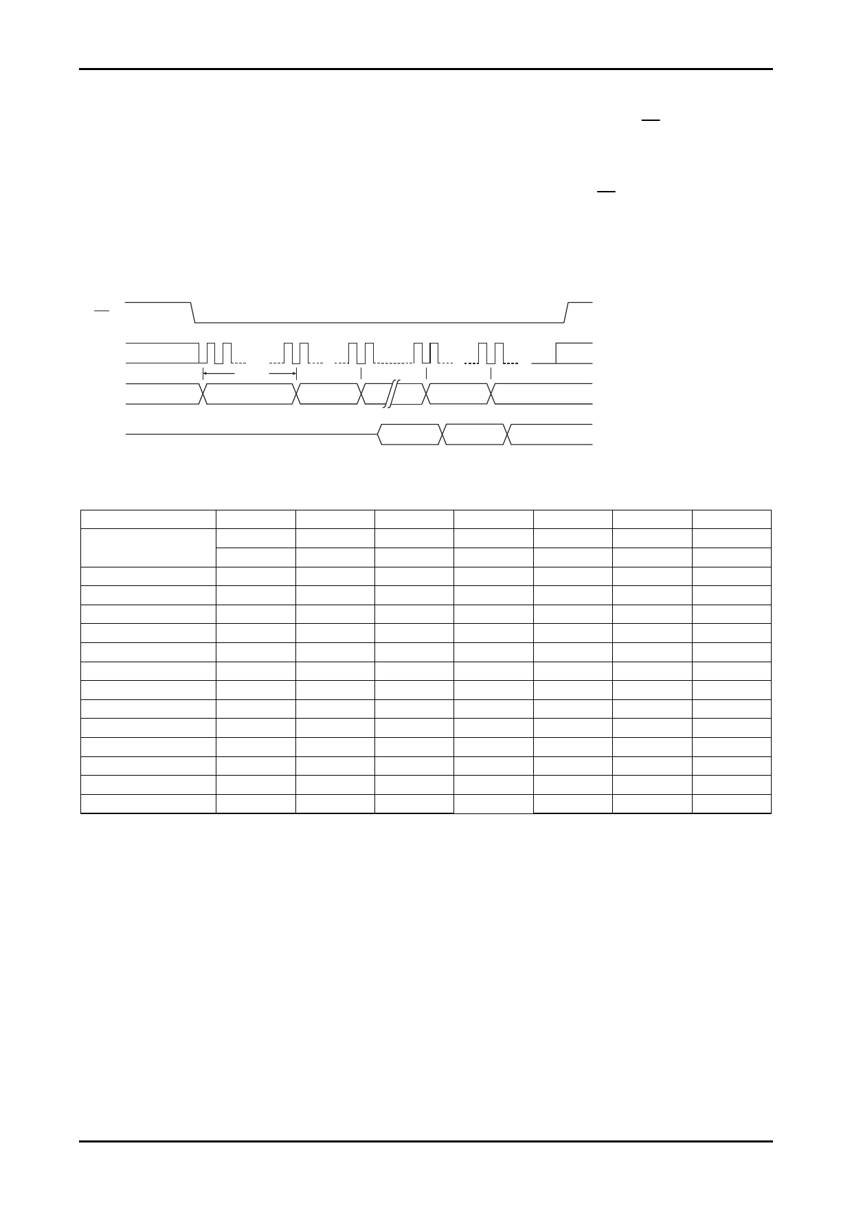
Figure 3 I/O waveforms
CS
SCK
Mode3
Mode0
SI
SO
MSB
(Bit7)
8CLK
Farst bass
second bass
LSB
(Bit0)
n bass
DATA
DATA
Table 2 Command Settings
Command
1st bus cycle 2nd bus cycle 3rd bus cycle 4th bus cycle 5th bus cycle
Read
03h
A23-A16
A15-A8
A7-A0
RD *1
0Bh
A23-A16
A15-A8
A7-A0
X
Small sector erase
20h / D7h
A23-A16
A15-A8
A7-A0
Sector erase
D8h
A23-A16
A15-A8
A7-A0
Chip erase
60h / C7h
Page program
02h
A23-A16
A15-A8
A7-A0
PD *2
Write enable
06h
Write disable
04h
Power down
B9h
Status register read
05h
Status register write
01h
DATA
Read silicon ID 1 *2
9Fh
Read silicon ID 2 *3
ABh
X
X
X
power down
B9h
Exit power down mode
ABh
Explanatory notes for Table 2
"X" signifies "don't care" (that is to say, any value may be input).
The "h" following each code indicates that the number given is in hexadecimal notation.
Addresses A23 to A19 for all commands are "Don't care".
*1: "RD" stands for read data. *2: "PD" stands for page program data.
6th bus cycle
RD *1
RD *1
PD *2
Nth bus cycle
RD *1
RD *1
PD *2
No.A1577-4/22
Share Link: 