LE25FS406 „Éá„Éľ„āŅ„ā∑„Éľ„Éą„ĀģŤ°®Á§ļÔľąPDFÔľČ - SANYO -> Panasonic
ťÉ®ŚďĀÁē™ŚŹ∑
„ā≥„É≥„ÉĚ„Éľ„Éć„É≥„ÉąŤ™¨śėé
„É°„Éľ„āę„Éľ
LE25FS406 Datasheet PDF : 22 Pages
| |||
LE25FS406
Description of Commands and Their Operations
A detailed description of the functions and operations corresponding to each command is presented below.
1. Standard SPI read
There are two read commands, the standard SPI read command and High-speed read command.
1-1. Read command
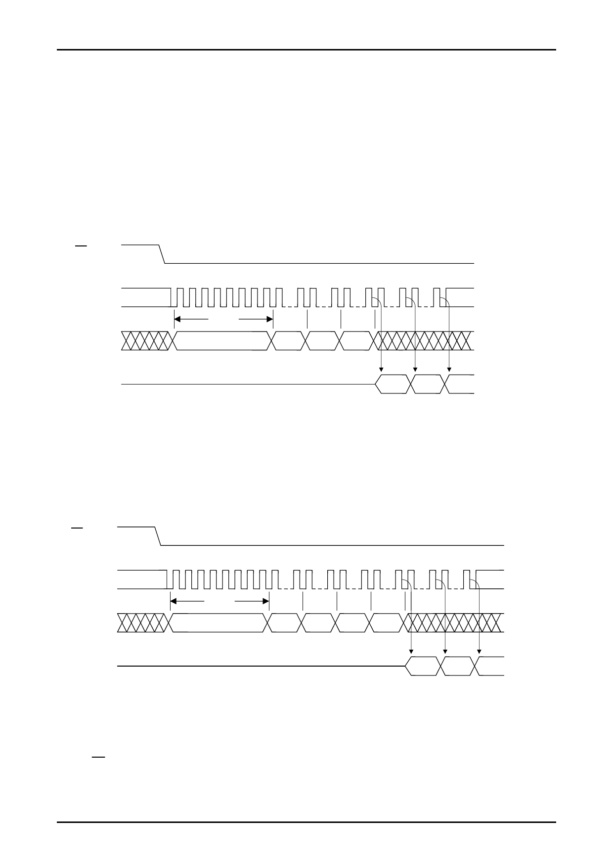
Consisting of the first through fourth bus cycles, the 4 bus cycle read command inputs the 24-bit addresses following
(03h). The data is output from SO on the falling clock edge of fourth bus cycle bit 0 as a reference. "Figure 4-a Read"
shows the timing waveforms.
Figure 5-a 4 Bus Read
CS
SCK
SI
Mode3
Mode0
0 1 2 3 4 5 6 7 8 15 16 23 24 31 32 39 40 47
8CLK
03h
Add. Add. Add.
SO
1-2. High-speed Read command
High Impedance
N
N+1 N+2
DATA DATA DATA
MSB MSB MSB
Consisting of the first through fifth bus cycles, the High-speed read command inputs the 24-bit addresses and 8 dummy
bits following (0Bh). The data is output from SO using the falling clock edge of fifth bus cycle bit 0 as a reference.
"Figure 4-b High-speed Read" shows the timing waveforms.
Figure 4-b High-speed Read
CS
SCK
SI
SO
Mode3
Mode0
0 1 2 3 4 5 6 7 8 15 16 23 24 31 32 39 40 47 48 55
8CLK
0Bh
MSB
Add. Add. Add.
High Impedance
X
N
N+1 N+2
DATA DATA DATA
MSB MSB MSB
When SCK is input continuously after the read command has been input and the data in the designated addresses has
been output, the address is automatically incremented inside the device while SCK is being input, and the corresponding
data is output in sequence. If the SCK input is continued after the internal address arrives at the highest address
(7FFFFh), the internal address returns to the lowest address (00000h), and data output is continued. By setting the logic
level of CS to high, the device is deselected, and the read cycle ends. While the device is deselected, the output pin SO
is in a high-impedance state.
No.A1577-6/22
Share Link: 