XC2735X データシートの表示(PDF) - Infineon Technologies
部品番号
コンポーネント説明
メーカー
XC2735X
Infineon Technologies

XC2735X Datasheet PDF : 101 Pages
| |||
XC2735X
XC2000 Family Derivatives / Base Line
General Device Information
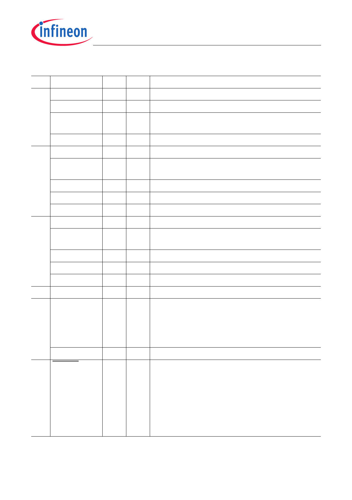
Table 5
Pin Definitions and Functions (cont’d)
Pin Symbol
Ctrl. Type Function
56 P10.13
O0 / I St/B Bit 13 of Port 10, General Purpose Input/Output
U1C0_DOUT O1 St/B USIC1 Channel 0 Shift Data Output
U1C0_SELO O3 St/B USIC1 Channel 0 Select/Control 3 Output
3
U1C0_DX0D I
St/B USIC1 Channel 0 Shift Data Input
58 P10.14
O0 / I St/B Bit 14 of Port 10, General Purpose Input/Output
U1C0_SELO O1 St/B USIC1 Channel 0 Select/Control 1 Output
1
U0C1_DOUT O2 St/B USIC0 Channel 1 Shift Data Output
ESR2_2
I
St/B ESR2 Trigger Input 2
U0C1_DX0C I
St/B USIC0 Channel 1 Shift Data Input
59 P10.15
O0 / I St/B Bit 15 of Port 10, General Purpose Input/Output
U1C0_SELO O1 St/B USIC1 Channel 0 Select/Control 2 Output
2
U0C1_DOUT O2 St/B USIC0 Channel 1 Shift Data Output
U1C0_DOUT O3 St/B USIC1 Channel 0 Shift Data Output
U0C1_DX1C I
St/B USIC0 Channel 1 Shift Clock Input
60 XTAL2
O Sp/M Crystal Oscillator Amplifier Output
61 XTAL1
ESR2_9
I
Sp/M Crystal Oscillator Amplifier Input
To clock the device from an external source, drive
XTAL1, while leaving XTAL2 unconnected.
Voltages on XTAL1 must comply to the core
supply voltage VDDIM.
I
St/B ESR2 Trigger Input 9
62 PORST
I
In/B Power On Reset Input
A low level at this pin resets the XC2735X
completely. A spike filter suppresses input pulses
<10 ns. Input pulses >100 ns safely pass the filter.
The minimum duration for a safe recognition
should be 120 ns.
An internal pullup device will hold this pin high
when nothing is driving it.
Data Sheet
21
V2.0, 2009-03
Share Link: