UPC494C(MS) データシートの表示(PDF) - NEC => Renesas Technology
部品番号
コンポーネント説明
メーカー
UPC494C(MS) Datasheet PDF : 20 Pages
| |||
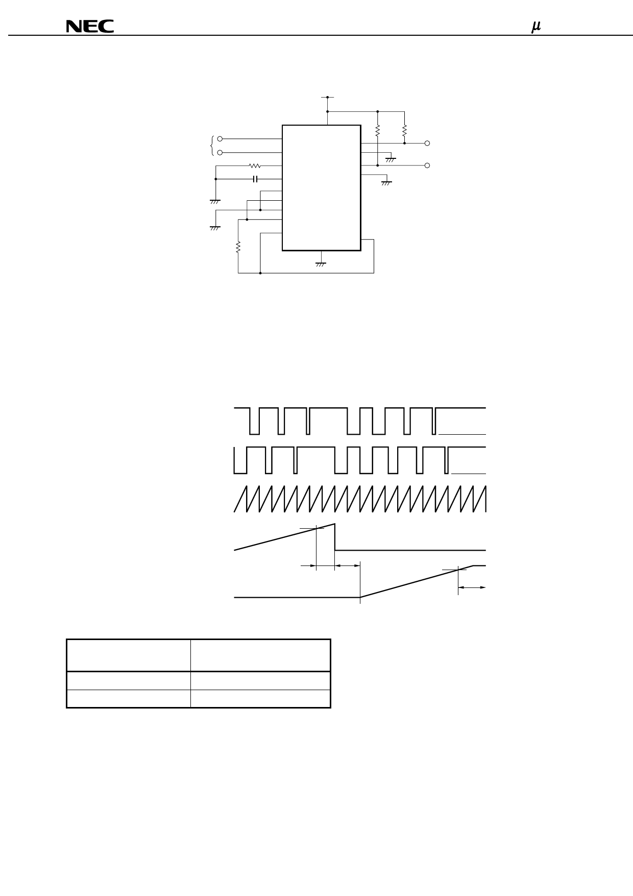
Figure1. Test Circuit
VCC = 15 V
(12)
RL
Test Input
(4) Dead-TimeVCC
(3) Control
Feed-Back
12 kΩ
(6)
RT
0.01µF Note
(5)
(1)
CT
(2)
(16)
(15)
Non-Inv. Input
Inv. Input
Non-Inv. Input
Inv. Input
150 Ω
C1
E1
(8)
(9)
2W
(11)
C2
E2
(10)
50 kΩ
(13)
Output Control
(14)
GND Ref Out
(7)
RL
150 Ω
2 W Output 1
Output 2
µPC494
Note Recommend film capacitor.
5 Caution When the emitter follower is output, connect C1 and C2 to VCC and E1 and E2 to
GND via RL.
Figure2. Voltage Waveform
C1 Output Voltage
C2 Output Voltage
CT Voltage
Dead-Time Control
Input
Threshold Voltage
Feed-Back Input
(E.A. Output) 0.7 V
0% MAX.
Threshold Voltage
VCC
0V
VCC
0V
0%
Connection of Output Control Pin (Pin No.13)
Output Control Input
(Pin No.13)
Operation Mode
At Ref Out
Normal push-pull operation
Grounded
Single-ended or parallel output
6
Data Sheet G12649EJ4V0DS00
Share Link: 