LC75741W(1995) データシートの表示(PDF) - SANYO -> Panasonic
部品番号
コンポーネント説明
メーカー
LC75741W Datasheet PDF : 10 Pages
| |||
LC75741E, 75741W
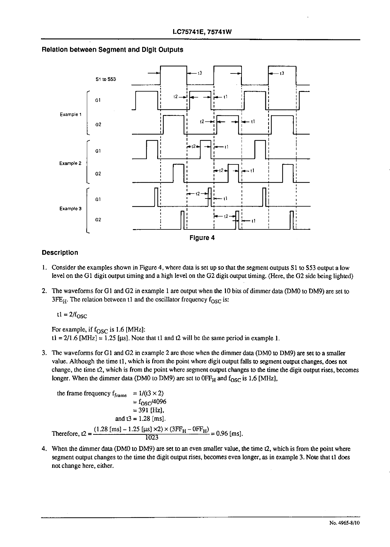
Relation between Segment and Digit Outputs
Figure 4
Description
1. Consider the examples shown in Figure 4, where data is set up so that the segment outputs S1 to S53 output a low
level on the G1 digit output timing and a high level on the G2 digit output timing. (Here, the G2 side being lighted)
2. The waveforms for G1 and G2 in example 1 are output when the 10 bits of dimmer data (DM0 to DM9) are set to
3FEH. The relation between t1 and the oscillator frequency fOSC is:
t1 = 2/fOSC
For example, if fOSC is 1.6 [MHz]:
t1 = 2/1.6 [MHz] = 1.25 [µs]. Note that t1 and t2 will be the same period in example 1.
3. The waveforms for G1 and G2 in example 2 are those when the dimmer data (DM0 to DM9) are set to a smaller
value. Although the time t1, which is from the point where digit output falls to segment output changes, does not
change, the time t2, which is from the point where segment output changes to the time the digit output rises, becomes
longer. When the dimmer data (DM0 to DM9) are set to 0FFH and fOSC is 1.6 [MHz],
the frame frequency fframe = 1/(t3 × 2)
= fOSC/4096
= 391 [Hz],
and t3 = 1.28 [ms].
Therefore,
t2
=
(1.28
[ms]
–
1.25
[µs] ×2)
1023
×
(3FFH
–
0FFH)
=
0.96
[ms].
4. When the dimmer data (DM0 to DM9) are set to an even smaller value, the time t2, which is from the point where
segment output changes to the time the digit output rises, becomes even longer, as in example 3. Note that t1 does
not change here, either.
No. 4965-8/10
Share Link: 