LC7574 データシートの表示(PDF) - SANYO -> Panasonic
部品番号
コンポーネント説明
メーカー
LC7574 Datasheet PDF : 10 Pages
| |||
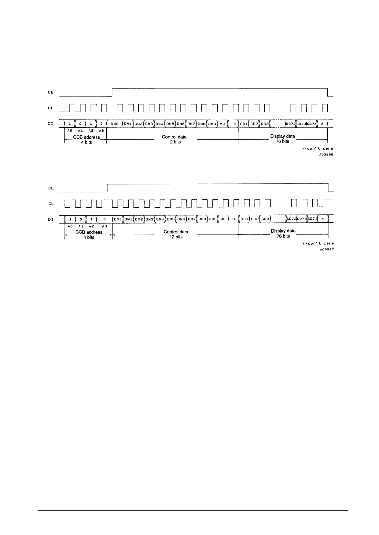
Serial Data Transfer Format
1. When CL is stopped at the low level
LC7574NE, 7574NW
2. When CL is stopped at the high level
Figure 2
CCB address: Transfer 1010B, as shown in Figure 2.
M0:
Digital/analog dimmer selection data
M0 = 0 ....................................Digital dimmer
M0 = 1 ....................................Analog dimmer
DM0 to DM9: Dimmer data
This data controls the duty of the G1 and G2 digit output pins when the digital dimmer is selected.
This data consists of 10 bits, of which DM0 is the LSB. Note that display intensity can be adjusted by
controlling the duty of the G1 and G2 digit output pins. (The DM0 to DM9 dimmer data is ignored
when the analog dimmer is selected.)
SD1 to SD74: Display data
SD1 to SD37...........................Display data for the G1 digit output pin
SD38 to SD74.........................Display data for the G2 digit output pin
SDn (n = 1 to 74) = 1..............Display on
SDn (n = 1 to 74) = 0..............Display off
T0:
Test data
The T0 bit must be set to 0.
No. 3586-5/10
Share Link: 