LT1074 データシートの表示(PDF) - Linear Technology
部品番号
コンポーネント説明
メーカー
LT1074 Datasheet PDF : 16 Pages
| |||
LT1074/LT1076
ELECTRICAL CHARACTERISTICS
Note 1: Absolute Maximum Ratings are those values beyond which the life
of a device may be impaired.
Note 2: To calculate maximum switch “on” voltage at currents between
low and high conditions, a linear interpolation may be used.
Note 3: A feedback pin voltage (VFB) of 2.5V forces the VC pin to its low
clamp level and the switch duty cycle to zero. This approximates the zero
load condition where duty cycle approaches zero.
Note 4: Total voltage from VIN pin to ground pin must be ≥ 8V after start-
up for proper regulation.
Note 5: Switch frequency is internally scaled down when the feedback pin
voltage is less than 1.3V to avoid extremely short switch on times. During
testing, VFB is adjusted to give a minimum switch on time of 1µs.
Note
6:
ILIM
≈
RLIM –
2k
1k
(LT1074),
ILIM ≈
RLIM – 1k
5.5k
(LT1076).
Note 7: Switch to input voltage limitation must also be observed.
Note 8: VMAX = 40V for the LT1074/76 and 60V for the LT1074HV/76HV.
Note 9: Does not include switch leakage.
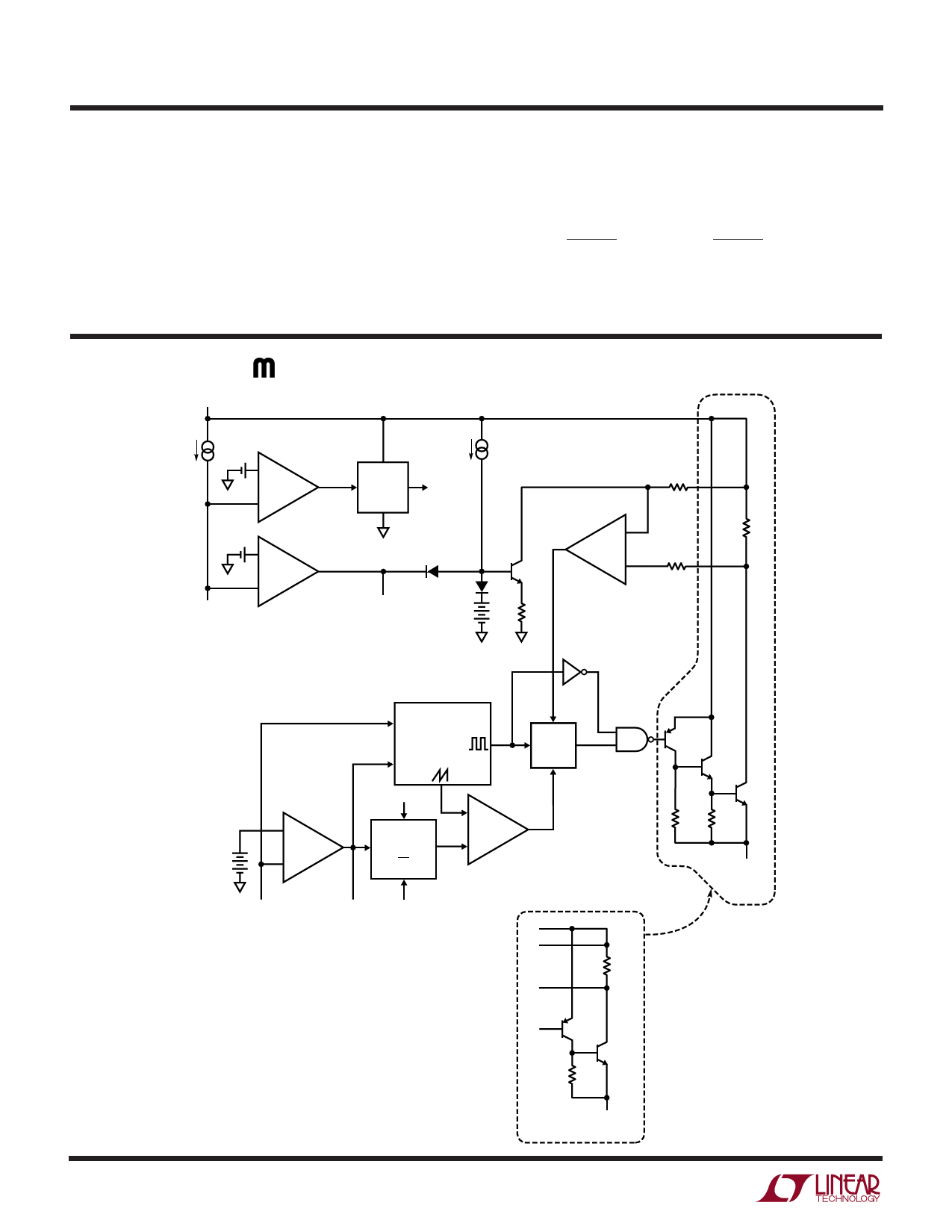
BLOCK DIAGRA
INPUT SUPPLY
LT1074
10µ A
0.3V
+
µ-POWER
SHUTDOWN
–
6V
REGULATOR
AND BIAS
320 µA
6V TO ALL
CIRCUITRY
2.35V
+
CURRENT
LIMIT
SHUTDOWN
500 Ω
CURRENT
LIMIT
COMP
+
0.04
C2
–
250 Ω
–
SHUTDOWN*
I LIM*
4.5V 10k
4
2.21V
+
A1
ERROR
AMP
–
FREQ SHIFT
100kHz
OSCILLATOR
SYNC
3V(p-p)
R
S
R/S
LATCH
Q
G1
R
VIN
Z
ANALOG
X
MULTIPLIER
XY
Z
Y
+
C1
–
PULSE WIDTH
COMPARATOR
FB
VC
24V (EQUIVALENT)
LT1076
*AVAILABLE ON PACKAGES WITH PIN
COUNTS GREATER THAN 5.
0.1 Ω
400 Ω 15 Ω
SWITCH
OUTPUT
(VSW)
100Ω
SWITCH
OUTPUT (VSW )
LT1074 • BD01
1074fd
Share Link: 