NJU6433B データシートの表示(PDF) - Japan Radio Corporation
部品番号
コンポーネント説明
メーカー
NJU6433B Datasheet PDF : 12 Pages
| |||
NJU6433B
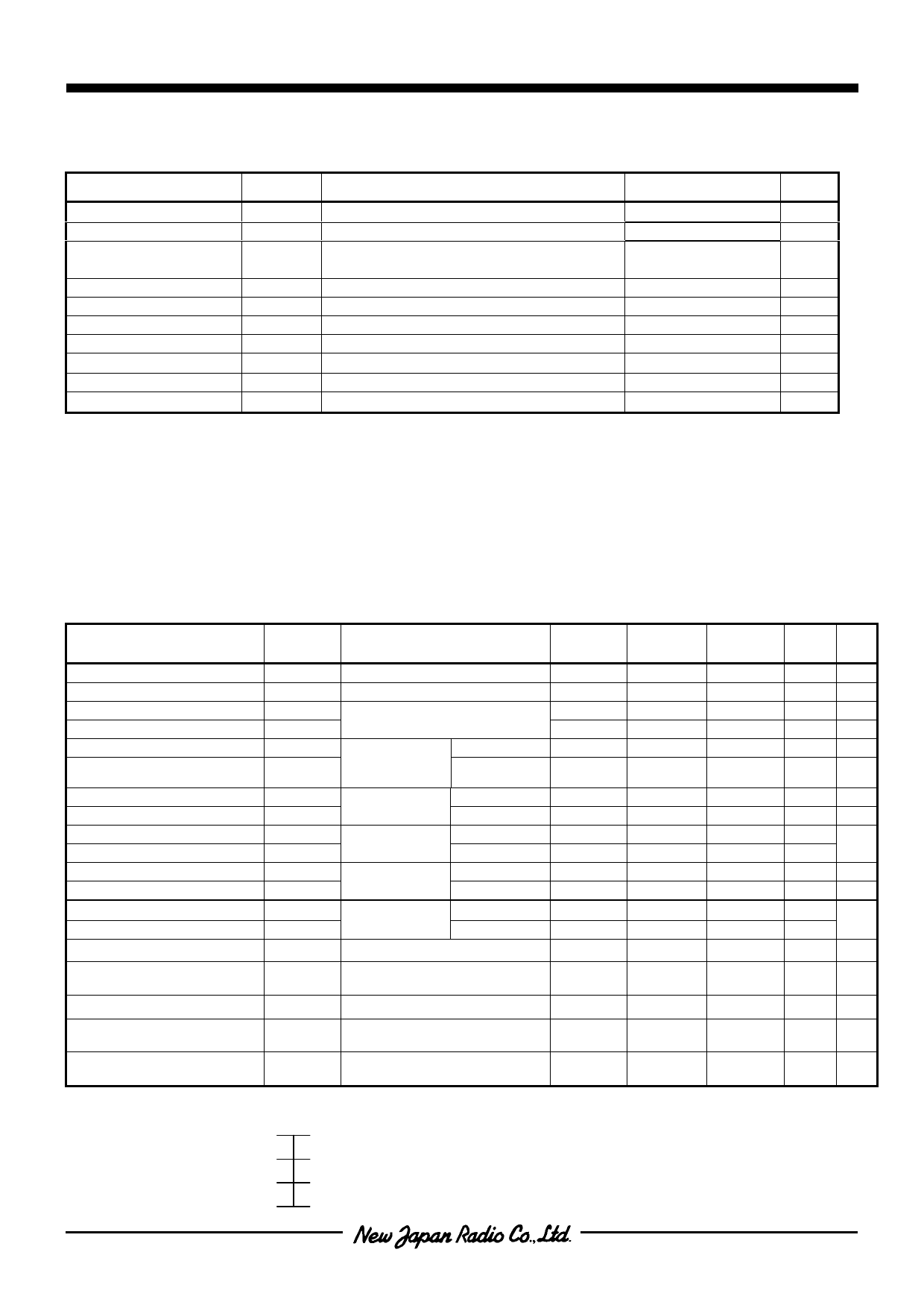
ABSOLUTE MAXIMUM RATINGS
PARAMETER
SYMBOL
CONDITIONS
RATINGS
Ta=25°C
UNIT
Operating Voltage (1)
VDDmax VDD Terminal, Ta=25°C
-0.3~+7.0
V
Operating Voltage (2)
VLCD
VDD-6.5~VSS
V
Input Voltage (1)
V1(1)
CE, SCL, DATA, MODE, INHb Terminals
Ta=25°C
-0.3~+7.0
V
Input Voltage (2)
V1(2) OSC1, OSC2 Terminals
-0.3~VDD+0.3
V
Output Voltage
V0
OSC1, OSC2 Terminals
-0.3~VDD+0.3
V
Output Current (1)
IO(1)
SEG1~SEG50 Terminals
100
uA
Output Current (2)
IO(2)
COM1~COM4 Terminals
1.0
mA
Power Dissipation
PDmax Ta=85°C
300
mW
Operating Temperature Topr
-30~+85
°C
Storage Temperature
Tstg
-40~+125
°C
Note 1) All voltage values are specified as VSS = 0V.
Note 2) If the LSI is used on condition above the absolute maximum ratings, the LSI may be destroyed. Using
the LSI within electrical characteristics is strongly recommended for normal operation. Use beyond the
electric characteristics conditions will cause malfunction and poor reliability.
Note 3) The relation VDD > VSS ≥ VLCD must be maintained.
Note 4) Decoupling capacitor should be connected between VDD and VSS due to the stabilized operation for the
LSI.
ELECTRICAL CHARACTERISTICS
• DC Characteristics
PARAMETER
SYMBOL
CONDITIONS
Operating Voltage (1)
Operating Voltage (2)
"H" Input Voltage
"L” Input Voltage
"H" Input Current
"L" Input Current
VDD
VLCD
VIH
VIL
VIH
VIL
VDD Terminal
VLCD Terminal
CE, SCL, DATA, MODE, INHb
CE,SCL,
DATA,MODE,
INHb
VI =VDD
VI =VSS
"H" Output Voltage (1)
"L” Output Voltage (1)
Middle Level Voltage 1/3(1)
Middle Level Voltage 2/3(1)
"H" Output Voltage (2)
"L" Output Voltage (2)
VOH(1)
VOL(1)
VMS1/3
VMS2/3
VOH(2)
VOL(2)
SEG1~SEG50
SEG1~SEG50
COM1~COM4
IO=-10uA
IO=+10uA
IO=±10uA
IO=±10uA
IO=-100uA
IO=+100uA
Middle Level Voltage 1/3(2)
Middle Level Voltage 2/3(2)
VMC1/3
VMC2/3
COM1~COM4
IO=±100uA
IO=±100uA
Oscillating Frequency Range
fRNG
OSC1, OSC2 Terminals
Oscillating Frequency
fOSC
OSC1, OSC2 Terminals
R=140kΩ, VDD=5V
Operating Current (1)
ISS
VSS Terminal, VDD=5V
Operating Current (2)
ILCD
VLCD Terminal,
VDD=5V, VLCD=VDD-6.5V
Hysteresis Voltage
VH
CE, SCL, DATA, MODE, INHb
VDD=5V
Note 1) V1=1/3|VDD-VLCD|, V2=2/3|VDD-VLCD|
(VDD=5V±10%, VLCD=VDD-6.5V, Ta=25°C)
MIN
2.4
VSS
0.7VDD
VSS
TYP
5.0
MAX
NO
UNIT
TE
5.5
V
VDD-6.5 V
VDD
V
0.3VDD
V
5
uA
5
uA
VDD-1.0
V1-1.0
V2-1.0
VDD-0.6
V1-0.6
V2-0.6
25
V
VLCD+1.0 V
V1
V2
V1+1.0
V2+1.0
V
V
1
V
VLCD+0.6 V
V1
V1+0.6
V
1
V2
V2+0.6 V
200 kHz
115
130
145 kHz
50
80
uA
15
25
uA
0.3
V
VDD
V2
2/3|VDD-VLCD|
V1
1/3|VDD-VLCD|
VLCD
Ver.2012-10-23
-9-
Share Link: 