MT46V16M16FG データシートの表示(PDF) - Micron Technology
部品番号
コンポーネント説明
メーカー
MT46V16M16FG Datasheet PDF : 80 Pages
| |||
256Mb: x4, x8, x16
DDR SDRAM
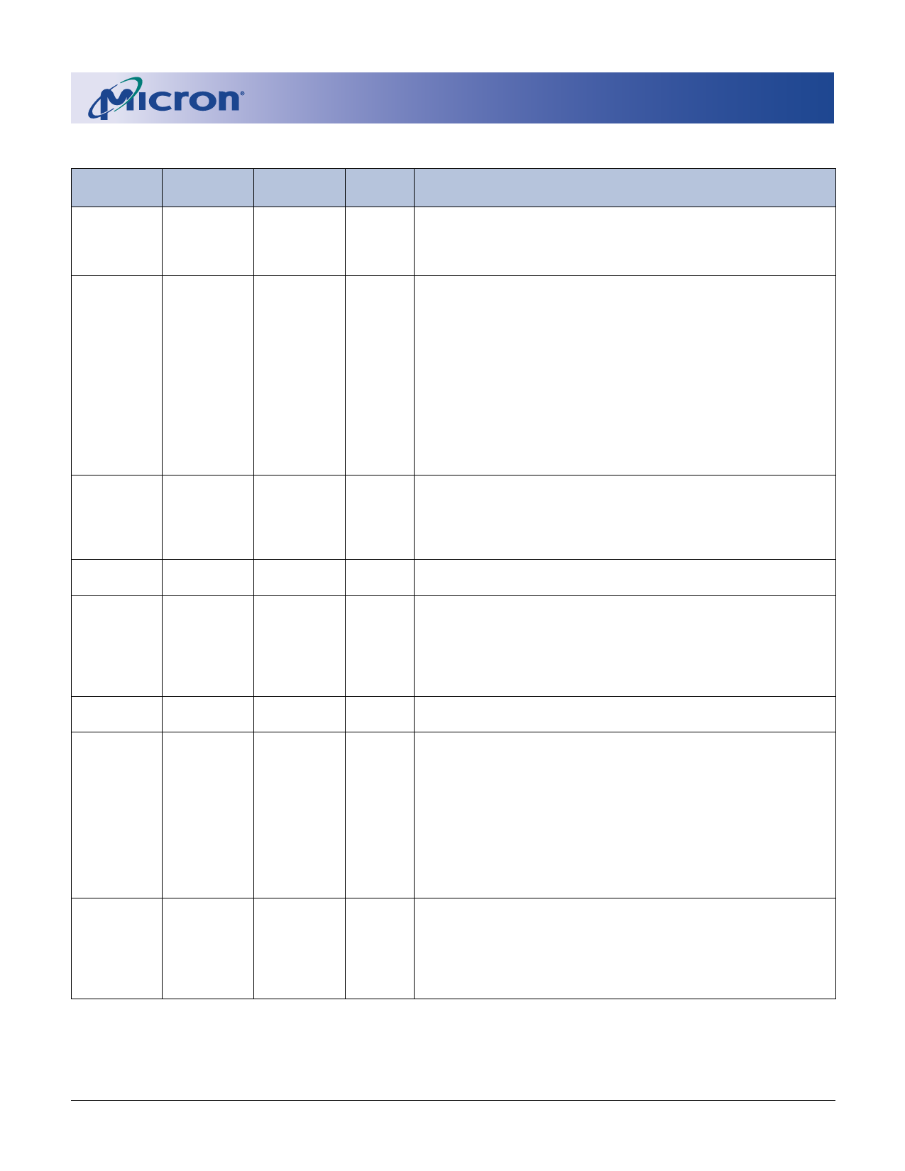
Table 2: Ball/Pin Descriptions
FBGA
NUMBERS
G2, G3
TSOP
NUMBERS
45, 46
SYMBOL
CK, CK#
H3
44
CKE
H8
24
CS#
H7, G8, G7
3F
F7, 3F
23, 22, 21
47
20, 47
RAS#, CAS#,
WE#
DM
LDM, UDM
J8, J7
26, 27
BA0, BA1
K7, L8, L7, 29, 30, 31, 32, A0, A1, A2,
M8, M2, L3, 35, 36, 37, 38, A3, A4, A5,
L2, K3, K2, J3, 39, 40, 28 A6, A7, A8,
K8,
41, 42 A9, A10, A11,
J2, H2
A12
A8, B9, B7,
2, 4, 5,
C9, C7, D9, 7, 8, 10,
D7, E9, E1, 11, 13, 54, 56,
D3, D1, C3, 57, 59, 60, 62,
C1, B3, B1, A2
63,
65
DQ0–DQ2
DQ3–DQ5
DQ6–DQ8
DQ9–DQ11
DQ12–DQ14
DQ15
TYPE
Input
Input
Input
Input
Input
Input
Input
I/O
DESCRIPTION
Clock: CK and CK# are differential clock inputs. All address and
control input signals are sampled on the crossing of the positive
edge of CK and the negative edge of CK#. Output data (DQ and
DQS) is referenced to the crossings of CK and CK#.
Clock Enable: CKE HIGH activates and CKE LOW deactivates the
internal clock, input buffers, and output drivers. Taking CKE LOW
provides PRECHARGE POWER-DOWN and SELF REFRESH operations
(all banks idle) or ACTIVE POWER-DOWN (row ACTIVE in any bank).
CKE is synchronous for POWER-DOWN entry and exit and for SELF
REFRESH entry. CKE is asynchronous for SELF REFRESH exit and for
disabling the outputs. CKE must be maintained HIGH throughout
read and write accesses. Input buffers (excluding CK, CK#, and CKE)
are disabled during POWER- DOWN. Input buffers (excluding CKE)
are disabled during SELF REFRESH. CKE is an SSTL_2 input but will
detect an LVCMOS LOW level after VDD is applied and until CKE is
first brought HIGH, after which it becomes an SSTL_2 input only.
Chip Select: CS# enables (registered LOW) and disables (registered
HIGH) the command decoder. All commands are masked when CS#
is registered HIGH. CS# provides for external bank selection on
systems with multiple banks. CS# is considered part of the
command code.
Command Inputs: RAS#, CAS#, and WE# (along with CS#) define
the command being entered.
Input Data Mask: DM is an input mask signal for write data. Input
data is masked when DM is sampled HIGH along with that input
data during a WRITE access. DM is sampled on both edges of DQS.
Although DM pins are input-only, the DM loading is designed to
match that of DQ and DQS pins. For the x16, LDM is DM for DQ0–
DQ7 and UDM is DM for DQ8–DQ15. Pin 20 is a NC on x4 and x8.
Bank Address Inputs: BA0 and BA1 define to which bank an
ACTIVE, READ, WRITE, or PRECHARGE command is being applied.
Address Inputs: Provide the row address for ACTIVE commands, and
the column address and auto precharge bit (A10) for READ/WRITE
commands, to select one location out of the memory array in the
respective bank. A10 sampled during a PRECHARGE command
determines whether the PRECHARGE applies to one bank (A10
LOW, bank selected by BA0, BA1) or all banks (A10 HIGH). The
address inputs also provide the op-code during a MODE REGISTER
SET command. BA0 and BA1 define which mode register (mode
register or extended mode register) is loaded during the LOAD
MODE REGISTER command.
Data Input/Output: Data bus for x16.
(DQ4–DQ15 are NC for the x4)
(DQ8–DQ16 are NC for the x8)
09005aef8076894f
256MBDDRx4x8x16_2.fm - Rev. F 6/03 EN
9
Micron Technology, Inc., reserves the right to change products or specifications without notice.
©2003 Micron Technology, Inc.
Share Link: 