AT24C08D データシートの表示(PDF) - Atmel Corporation
部品番号
コンポーネント説明
メーカー
AT24C08D Datasheet PDF : 28 Pages
| |||
4. Memory Organization
The AT24C08D is internally organized as 64 pages of 16 bytes each.
4.1 Device Addressing
Accessing the device requires an 8-bit Device Address word following a Start condition to enable the device for a
Read or Write operation. Since multiple slave devices can reside on the serial bus, each slave device must have its
own unique address so the Master can access each device independently.
The most significant four bits of the Device Address word is referred to as the device type identifier. The device
type identifier ‘1010’ (Ah) is required in bits seven through four of the Device Address byte (see Table 4-1).
Following the 4-bit device type identifier is the hardware slave address bit, A2. This bit can be used to expand the
address space by allowing up to two 8-Kbit Serial EEPROM devices on the same bus. The A2 value must correlate
with the voltage level on the corresponding hardwired input pins A2.
The A2 pin uses an internal proprietary circuit that automatically biases it to a Logic 0 state if the pin is allowed to
float. In order to operate in a wide variety of application environments, the pull-down mechanism is intentionally
designed to be somewhat strong. Once the pin is biased above the CMOS input buffer’s trip point (~0.5 x VCC), the
pull-down mechanism disengages. Atmel recommends connecting the A2 pin to a known state whenever possible.
When using the SOT23 and WLCSP packages, the A2 pin is not accessible and is left floating. The previously
mentioned automatic pull-down circuit will set this pin to a Logic 0 state. As a result, to properly communicate with
the device in the SOT23 and WLCSP packages, the A2 software bit must always be set to Logic 0 for any
operation.
Following the A2 hardware slave address bit are bits A9 and A8 (bit 2 and bit 1 of the Device Address byte), which
are the two most significant bits of the memory array word address. Please refer to Table 4-1 to review these bit
positions.
The eighth bit (bit 0) of the Device Address byte is the Read/Write operation select bit. A Read operation is initiated
if this bit is high and a Write operation is initiated if this bit is low.
Upon the successful comparison of the Device Address byte, the EEPROM will return an ACK. If a valid
comparison is not made, the device will NACK and return to a standby state.
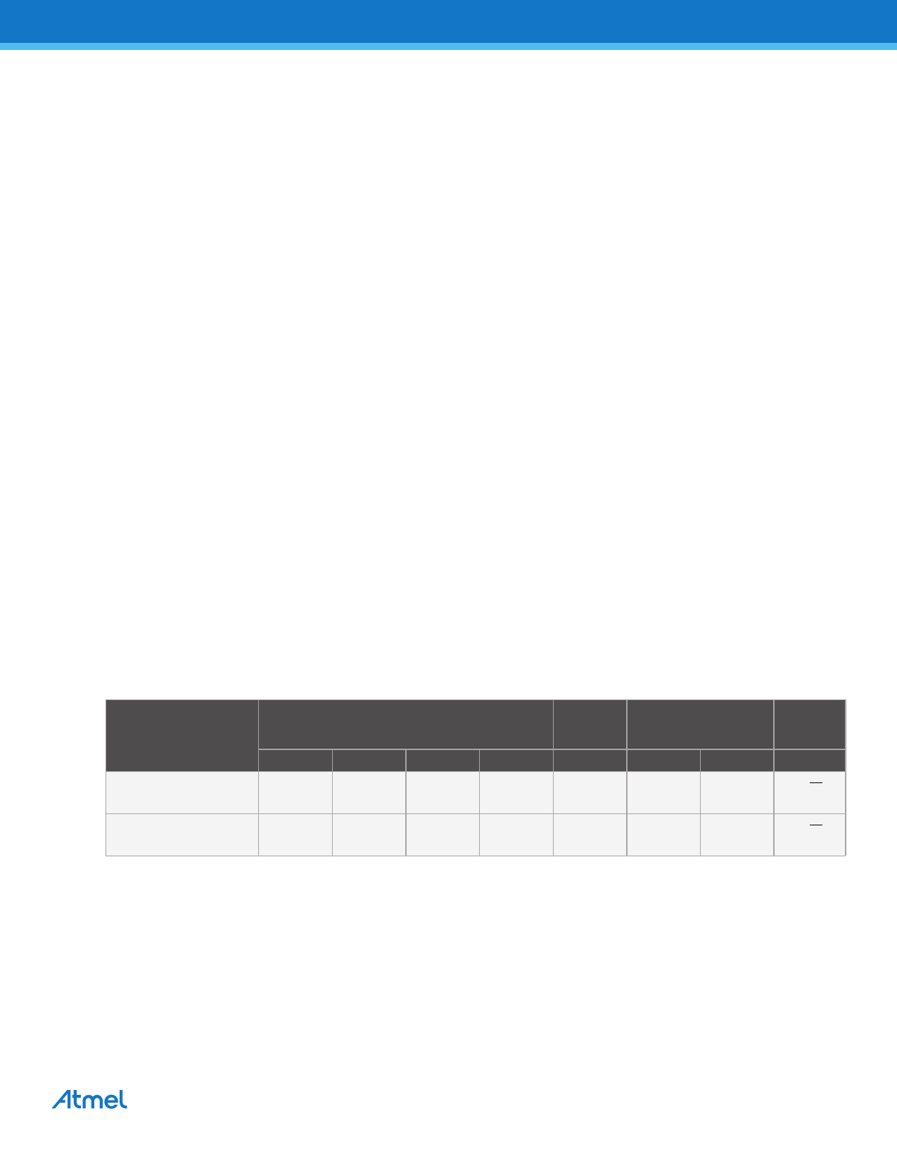
Table 4-1. Device Address Byte
Package
SOIC, TSSOP, UDFN,
PDIP, VFBGA
Bit 7
1
Device Type Identifier
Bit 6
Bit 5
0
1
Bit 4
0
Hardware
Slave
Address Bit
Bit 3
Most Significant Bits
of the Word Address
Bit 2
Bit 1
Read/ Write
Bit 0
A2
A9
A8
R/W
SOT23, WLCSP
1
0
1
0
0
A9
A8
R/W
AT24C08D [DATASHEET]
7
Atmel-8880B-SEEPROM-AT24C08D-Datasheet_042014
Share Link: 