ICX252 データシートの表示(PDF) - Sony Semiconductor
部品番号
コンポーネント説明
メーカー
ICX252 Datasheet PDF : 46 Pages
| |||
CXD3406GA
Detailed Description of Each Data
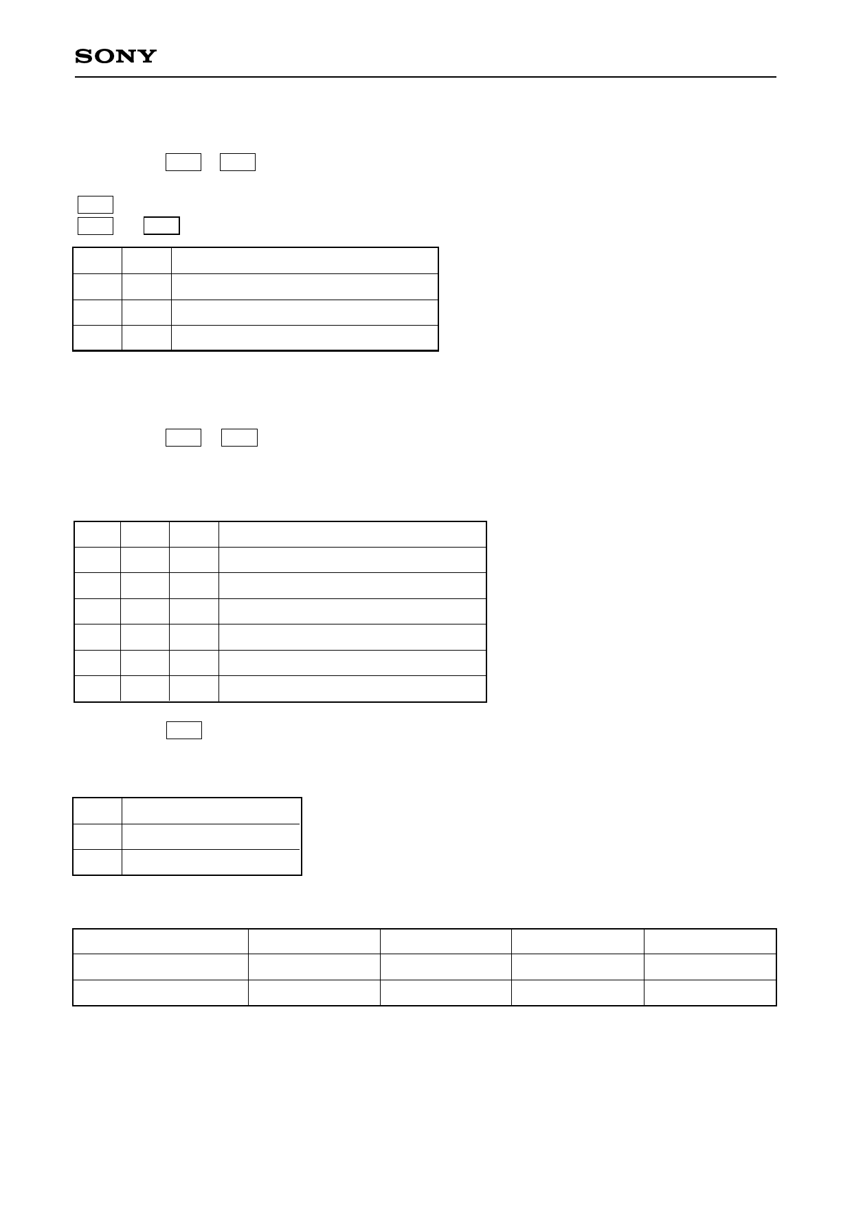
Shared data: D08 to D09 CTG [Category]
Of the data provided to the CXD3406GA by the timing generator block serial interface, the CXD3406GA loads
D10 and subsequent data to each data register as shown in the table below according to the combination of
D08 and D09 .
D09 D08
Description of operation
0
0 Loading to control data register
0
1 Loading to shutter data register
1
X Test mode
Note that the CXD3406GA can apply these categories consecutively within the same vertical period. However,
care should be taken as the data is overwritten if the same category is applied.
Control data: D10 to D12 MODE [Drive mode]
The CXD3406GA timing generator block drive mode can be switched as follows. However, the drive mode bits
are loaded to the CXD3406GA and reflected at the falling edge of VD.
D12 D11 D10
Description of operation
0
0
0 Draft mode (sextuple speed: default)
0
0
1 Frame mode (A field readout)
0
1
0 Frame mode (B Field readout)
0
1
1 Frame mode
1
0
X AF1 mode
1
1
X AF2 mode
Control data: D15 PTSG [Internal SSG output pattern]
The CXD3406GA internal SSG output pattern can be switched as follows. However, the drive mode bits are
loaded to the CXD3406GA and reflected at the falling edge of VD.
D15 Description of operation
0 NTSC equivalent pattern
1 PAL equivalent pattern
The VD period in each pattern is defined as follows for each drive mode.
Frame mode
NTSC equivalent pattern
PAL equivalent pattern
918H + 1716ck
945H∗1
∗1 Only 944H and 945H are 1208ck period.
Draft mode
262H + 1144ck
314H + 1568ck
AF1 mode
131H + 572ck
157H + 784ck
AF2 mode
65H + 1430ck
78H + 1536ck
See the Timing Charts for the actual operation.
– 22 –
Share Link: 