ICX252 データシートの表示(PDF) - Sony Semiconductor
部品番号
コンポーネント説明
メーカー
ICX252 Datasheet PDF : 46 Pages
| |||
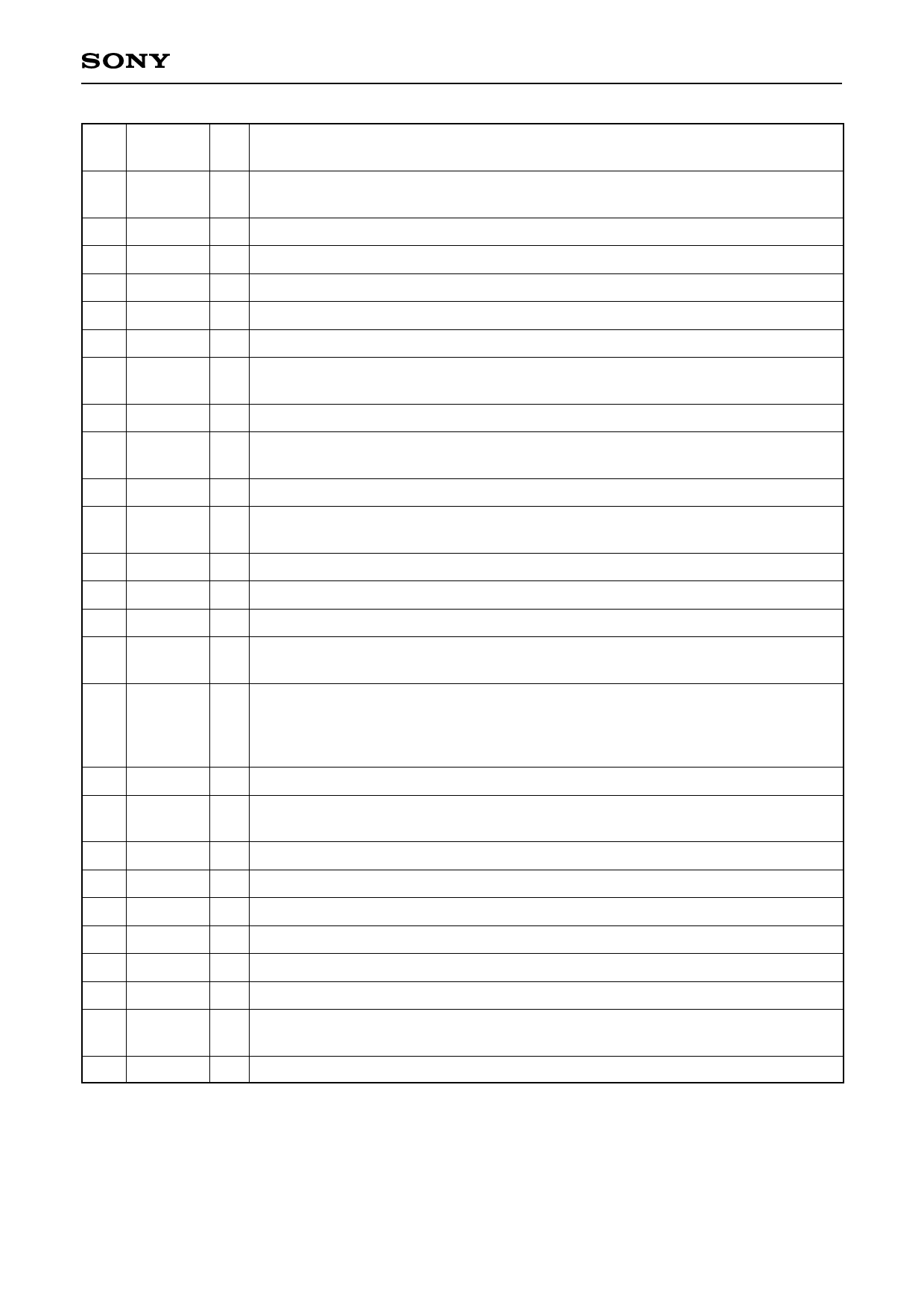
CXD3406GA
Pin
No.
Symbol
L2 SSI1
L3 VSS4
L4 VM
L5 V1A
L6 V3A
L7 VSS1
L8 SSGSL
L9 VDD1
M1 SCK1
M2 VD
M3 TEST1
M4 V2
M5 VH
M6 VL
M7 TEST2
M8 RST
M9 WEN
N1 SEN1
N2 HD
N3 VSS6
N4 V4
N5 V1B
N6 V3B
N7 SUB
N8 SNCSL
N9 ID
I/O
Description
I
Timing generator block serial interface data input.
Schmitt trigger input/No protective diode on power supply side.
— Timing generator block digital GND.
— Timing generator block digital GND. (GND for vertical driver)
O CCD vertical register clock output.
O CCD vertical register clock output.
— Timing generator block digital GND.
I
Internal SSG enable.
High: Internal SSG valid, Low: External SYNC valid
(With pull-down resistor)
— Timing generator block digital power supply.(Power supply for common logic block)
I
Timing generator block serial interface clock input.
Schmitt trigger input/No protective diode on power supply side.
I/O Vertical sync signal input/output.
I
Timing generator block test input 1.
Normally fix to GND.
(With pull-down resistor)
O CCD vertical register clock output.
— Timing generator block 15.0V power supply. (Power supply for vertical driver)
— Timing generator block –7.5V power supply. (Power supply for vertical driver)
I
Timing generator block test input 2.
Normally fix to GND.
(With pull-down resistor)
Timing generator block reset input.
I
High: Normal operation, Low: Reset control
Normally apply reset during power-on.
Schmitt trigger input/No protective diode on power supply side
O Memory write timing pulse output.
I
Timing generator block serial interface strobe input.
Schmitt trigger input/No protective diode on power supply side
I/O Horizontal sync signal input/output.
— Timing generator block digital GND.
O CCD vertical register clock output.
O CCD vertical register clock output.
O CCD vertical register clock output.
O CCD electronic shutter pulse output.
I
Control input used to switch sync system.
High: CKI sync, Low: MCKO sync
(With pull-down resistor)
O Vertical direction line identification pulse output.
–6–
Share Link: 