MP1482 データシートの表示(PDF) - Monolithic Power Systems
部品番号
コンポーネント説明
メーカー
MP1482 Datasheet PDF : 12 Pages
| |||
MP1482 – 2A, 18V SYNCHRONOUS RECTIFIED, STEP-DOWN CONVERTER
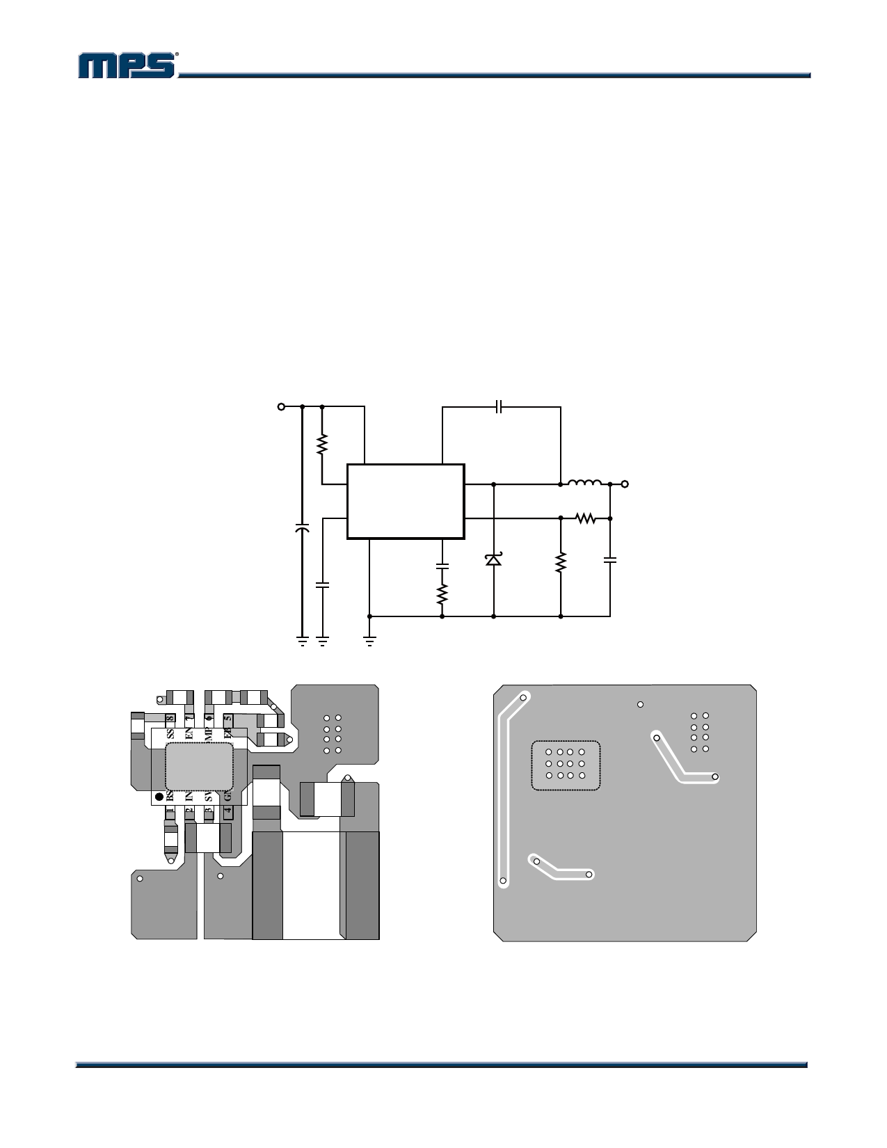
PCB LAYOUT GUIDE
PCB layout is very important to achieve stable
operation. It is highly recommended to duplicate
EVB layout for optimum performance.
If change is necessary, please follow these
guidelines and take Figure 4 for reference.
1) Keep the path of switching current short and
minimize the loop area formed by input cap,
high-side MOSFET and low-side MOSFET.
INPUT
4.75V to 18V
2) Bypass ceramic capacitors are suggested
to be put close to the Vin Pin.
3) Ensure all feedback connections are short
and direct. Place the feedback resistors
and compensation components as close to
the chip as possible.
4) Route SW away from sensitive analog
areas such as FB.
5) Connect IN, SW, and especially GND
respectively to a large copper area to cool
the chip to improve thermal performance
and long-term reliability.
C5
R4
2
7 IN
EN
1
BS 3
SW
L1
OUTPUT
MP1482
8
5
R1
C1
SS
GND
FB
COMP
4
C4
6
C3
D1
R2
C2
(optional)
R3
MP1482 Typical Application Circuit
R4
C3
R3
C4
R21
R1
PGND
PGND
D1
C2
SGND
C5
C1
L1
Top Layer
Bottom Layer
Figure 4—MP1482 Typical Application Circuit and PCB Layout Guide
MP1482 Rev. 1.31
www.MonolithicPower.com
11
7/9/2012
MPS Proprietary Information. Patent Protected. Unauthorized Photocopy and Duplication Prohibited.
© 2012 MPS. All Rights Reserved.
Share Link: 