CXA1998BQ データシートの表示(PDF) - Sony Semiconductor
部品番号
コンポーネント説明
メーカー
CXA1998BQ Datasheet PDF : 28 Pages
| |||
CXA1998BQ
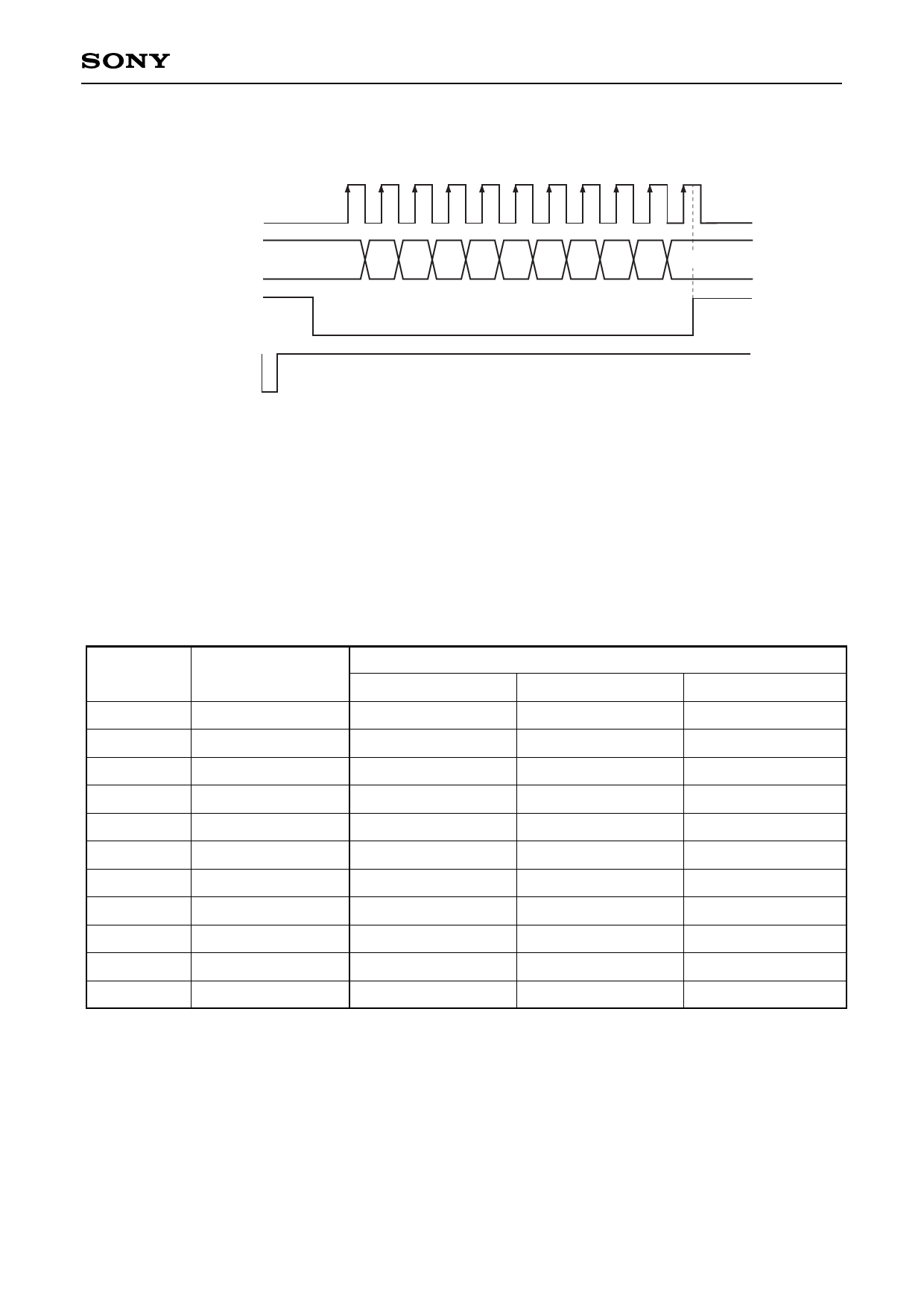
2. 11-bit serial data interface
CLK
(Pin 25)
DATA
(Pin 26)
LATCH
(Pin 24)
XRESET
(Pin 27)
D1 D2 D3 D4 D5 D6 D7 D8 D9 D10 D11
• The DATA signal is taken in at the rising edge of the CLK signal.
• The DATA signal is taken into the internal shift register when the LATCH signal is low. (Outputs (Pins 15 to 22)
hold the previous value while the LATCH signal is low.)
• The internal shift register data is latched and output in parallel at the rising edge of the LATCH signal.
(Internal shift register data is loaded while the LATCH signal is high.)
• The CLK signal of the 11th bit should fall after the LATCH signal rises.
• Reset is done when the XRESET pin is low. (asynchronous method)
Outputs (Pins 15 to 22) are all high (open) during reset.
DATA
(Pin 26)
D1
D2
D3
D4
D5
D6
D7
D8
D9
D10
D11
Control signal
M2
M1
PL2
PL1
BPB
BPA
PB MUTE
AGC OFF
SPEED
DECK AB
REC MUTE
Output pin
Pin 22
Pin 21
Pin 20
Pin 19
Pin 18
Pin 17
—
—
Pin 16
—
Pin 15
Output
Input set at low
Low
Low
Low
Low
Low
Low
Low mute OFF
AGC function stops
Low, normal speed
DECK A selected
Low mute OFF
Input set at high
High (OPEN)
High (OPEN)
High (OPEN)
High (OPEN)
High (OPEN)
High (OPEN)
High mute ON
AGC function operates
High (open) 1.7
DECK B selected
High (open) mute ON
– 18 –
Share Link: 