LTC6803 データシートの表示(PDF) - Linear Technology
部品番号
コンポーネント説明
メーカー
LTC6803 Datasheet PDF : 40 Pages
| |||
LTC6803-1/LTC6803-3
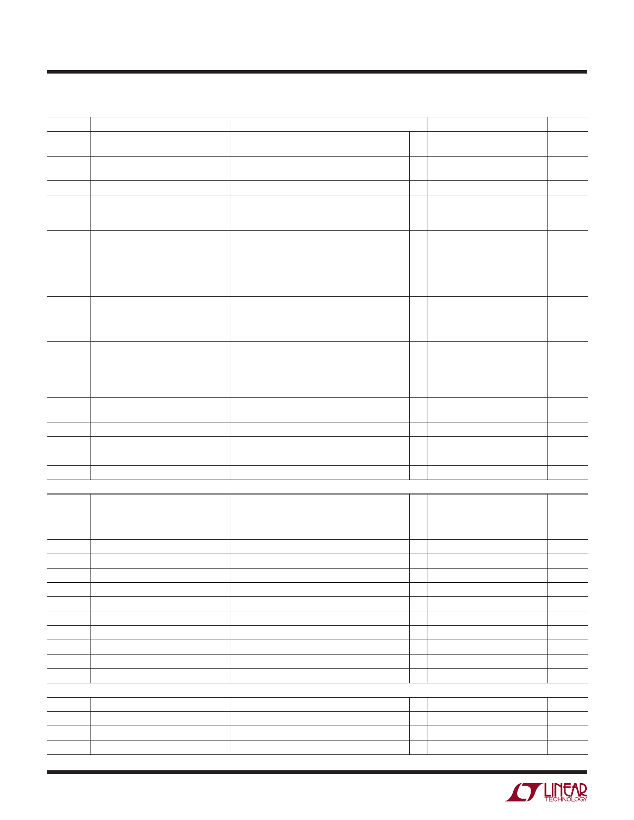
ELECTRICAL CHARACTERISTICS The l denotes the specifications which apply over the full operating
temperature range, otherwise specifications are at TA = 25°C. V+ = 43.2V, V– = 0V, unless otherwise noted.
SYMBOL PARAMETER
CONDITIONS
MIN
TYP
MAX
UNITS
VREF2
VREG
2nd Reference Voltage
Regulator Pin Voltage
Regulator Pin Short-Circuit Limit
10V < V+ < 50V, No Load
ILOAD = 4mA
2.25
2.5
2.75
V
l 2.1
2.5
2.9
V
l 4.5
5.0
5.5
V
l 4.5
5.0
V
l
8
mA
IB
Input Bias Current
In/Out of Pins C1 Through C12
When Measuring Cell
When Not Measuring Cell
–10
10
µA
1
nA
IS
Supply Current, Measure Mode
Current Into the V+ Pin When Measuring
(Note 7)
Continuous Measuring (CDC = 2)
620
780
1000
µA
Continuous Measuring (CDC = 2)
l 600
780
1150
µA
Measure Every 130ms (CDC = 5)
l 190
250
360
µA
Measure Every 500ms (CDC = 6)
l 140
175
250
µA
Measure Every 2 Seconds (CDC = 7)
l 55
70
105
µA
IQS
Supply Current, Standby
Current Into V+ Pin When In Standby, All Serial
8
12
16.5
µA
Port Pin at Logic “1”
LTC6803IG
l
6
12
18
µA
LTC6803HG
l
6
12
19
µA
ICS
Supply Current, Serial I/O
Current Into V+ Pin During Serial
3.1
3.9
4.3
mA
Communications, All Serial Port Pins at Logic “0”.
VMODE = “0”, This Current is Added to IS or IQS
LTC6803IG
l
3
3.9
4.5
mA
LTC6803HG
l
3
3.9
4.9
mA
ISD
Supply Current, Hardware Shutdown Current Out of V–, VC12 = 43.2V, V+ Floating
l
(Note 8)
0.001
1
µA
Discharge Switch-On Resistance
VCELL > 3V (Note 3)
IOW
Current Used for Open-Wire Detection
Thermal Shutdown Temperature
l 10
20
Ω
l 70
110
140
µA
145
°C
Thermal Shutdown Hysteresis
5
°C
Voltage Mode Timing Specifications
tCYCLE
Measurement Cycling
Time Required to Measure 12 Cells
l 11
13
15
ms
Time Required to Measure 10 Cells
l
9
11
13
ms
Time Required to Measure 3 Temperatures
l 2.8
3.4
4.1
ms
Time Required to Measure 1 Cell or Temperature l 1.0
1.2
1.4
ms
t1
SDI Valid to SCKI Rising Setup
t2
SDI Valid to SCKI Rising Hold
t3
SCKI Low
t4
SCKI High
t5
CSBI Pulse Width
t6
CSBI Falling to SCKI Rising
t7
CSBI Falling to SDO Valid
t8
SCKI Falling to SDO Valid
Clock Frequency
l 10
l 250
l 400
l 400
l 400
l 100
l 100
l
l
ns
ns
ns
ns
ns
ns
ns
250
ns
1
MHz
Watchdog Timer Timeout Period
l
1
2.5
Seconds
Timing Specifications
tPD1
CSBI to CSBO
tPD2
SCKI to SCKO
tPD3
SDI to SDOI Write Delay
tPD4
SDI to SDOI Read Delay
CCSBO = 150pF
CSCKO = 150pF
CSDOI = 150pF
CSDO = 150pF
l
600
ns
l
300
ns
l
300
ns
l
300
ns
680313f
4
Share Link: 