AM29F200BB-50 データシートの表示(PDF) - Advanced Micro Devices
部品番号
コンポーネント説明
メーカー
AM29F200BB-50
Advanced Micro Devices

AM29F200BB-50 Datasheet PDF : 40 Pages
| |||
DEVICE BUS OPERATIONS
This section describes the requirements and use of the
device bus operations, which are initiated through the
internal command register. The command register
itself does not occupy any addressable memory loca-
tion. The register is composed of latches that store the
commands, along with the address and data informa-
tion needed to execute the command. The contents of
the register serve as inputs to the internal state
machine. The state machine outputs dictate the func-
tion of the device. The appropriate device bus
operations table lists the inputs and control levels
required, and the resulting output. The following sub-
sections describe each of these operations in further
detail.
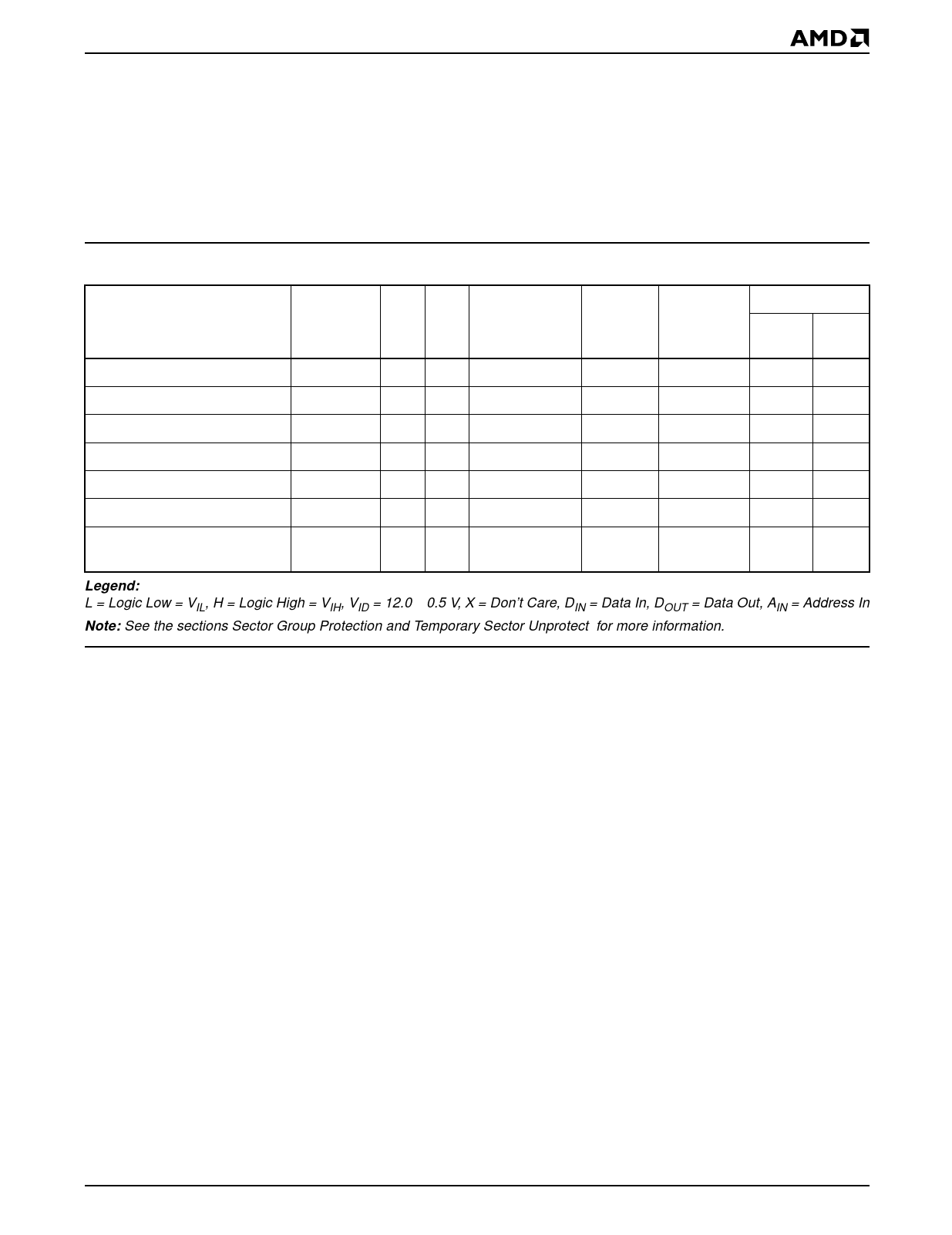
Table 1. Am29F200B Device Bus Operations
DQ8–DQ15
Operation
Read
Write
CMOS Standby
TTL Standby
Output Disable
CE#
OE# WE#
L
LH
L
HL
VCC ± 0.5 V X
X
H
XX
L
HH
RESET#
H
H
VCC ± 0.5 V
H
H
A0–A16
AIN
AIN
X
X
X
DQ0–DQ7
DOUT
DIN
High-Z
High-Z
High-Z
BYTE# BYTE#
= VIH = VIL
DOUT High-Z
DIN High-Z
High-Z High-Z
High-Z High-Z
High-Z High-Z
Hardware Reset
X
XX
L
X
High-Z High-Z High-Z
Temporary Sector Unprotect
(See Note)
X
XX
VID
AIN
DIN
DIN
X
Legend:
L = Logic Low = VIL, H = Logic High = VIH, VID = 12.0 ± 0.5 V, X = Don’t Care, DIN = Data In, DOUT = Data Out, AIN = Address In
Note: See the sections Sector Group Protection and Temporary Sector Unprotect for more information.
Word/Byte Configuration
The BYTE# pin controls whether the device data I/O
pins DQ15–DQ0 operate in the byte or word configura-
tion. If the BYTE# pin is set at logic ‘1’, the device is in
word configuration, DQ15–DQ0 are active and con-
trolled by CE# and OE#.
If the BYTE# pin is set at logic ‘0’, the device is in byte
configuration, and only data I/O pins DQ0–DQ7 are
active and controlled by CE# and OE#. The data I/O
pins DQ8–DQ14 are tri-stated, and the DQ15 pin is
used as an input for the LSB (A-1) address function.
Requirements for Reading Array Data
To read array data from the outputs, the system must
drive the CE# and OE# pins to VIL. CE# is the power
control and selects the device. OE# is the output
control and gates array data to the output pins. WE#
should remain at VIH. On x16 (word-wide) devices, the
BYTE# pin determines whether the device outputs
array data in words or bytes.
The internal state machine is set for reading array data
upon device power-up, or after a hardware reset. This
ensures that no spurious alteration of the memory
content occurs during the power transition. No
command is necessary in this mode to obtain array
data. Standard microprocessor read cycles that assert
valid addresses on the device address inputs produce
valid data on the device data outputs. The device
remains enabled for read access until the command
register contents are altered.
See “Reading Array Data” for more information. Refer
to the AC Read Operations table for timing specifica-
tions and to the Read Operations Timings diagram for
the timing waveforms. ICC1 in the DC Characteristics
table represents the active current specification for
reading array data.
Writing Commands/Command Sequences
To write a command or command sequence (which
includes programming data to the device and erasing
sectors of memory), the system must drive WE# and
CE# to VIL, and OE# to VIH.
On x16 (word-wide) devices, for program operations,
the BYTE# pin determines whether the device accepts
program data in bytes or words. Refer to “Word/Byte
Configuration” for more information.
Am29F200B
9
Share Link: