TC1015EV データシートの表示(PDF) - TelCom Semiconductor, Inc
部品番号
コンポーネント説明
メーカー
TC1015EV Datasheet PDF : 6 Pages
| |||
300mA CMOS LDO
TC1108
ABSOLUTE MAXIMUM RATINGS*
Input Voltage .............................................................. 6.5V
Output Voltage ........................... (VSS – 0.3) to (VIN + 0.3)
Power Dissipation .................... Internally Limited (Note 7)
Operating Temperature .................... – 40°C < TJ < 125°C
Storage Temperature ............................ – 65°C to +150°C
Maximum Voltage on Any Pin ........... VIN + 0.3V to – 0.3V
Lead Temperature (Soldering, 10 Sec.) ................ +260°C
*Absolute Maximum Ratings indicate device operation limits beyond dam-
age may occur. Device operation beyond the limits listed in Electrical
Characteristics is not recommended.
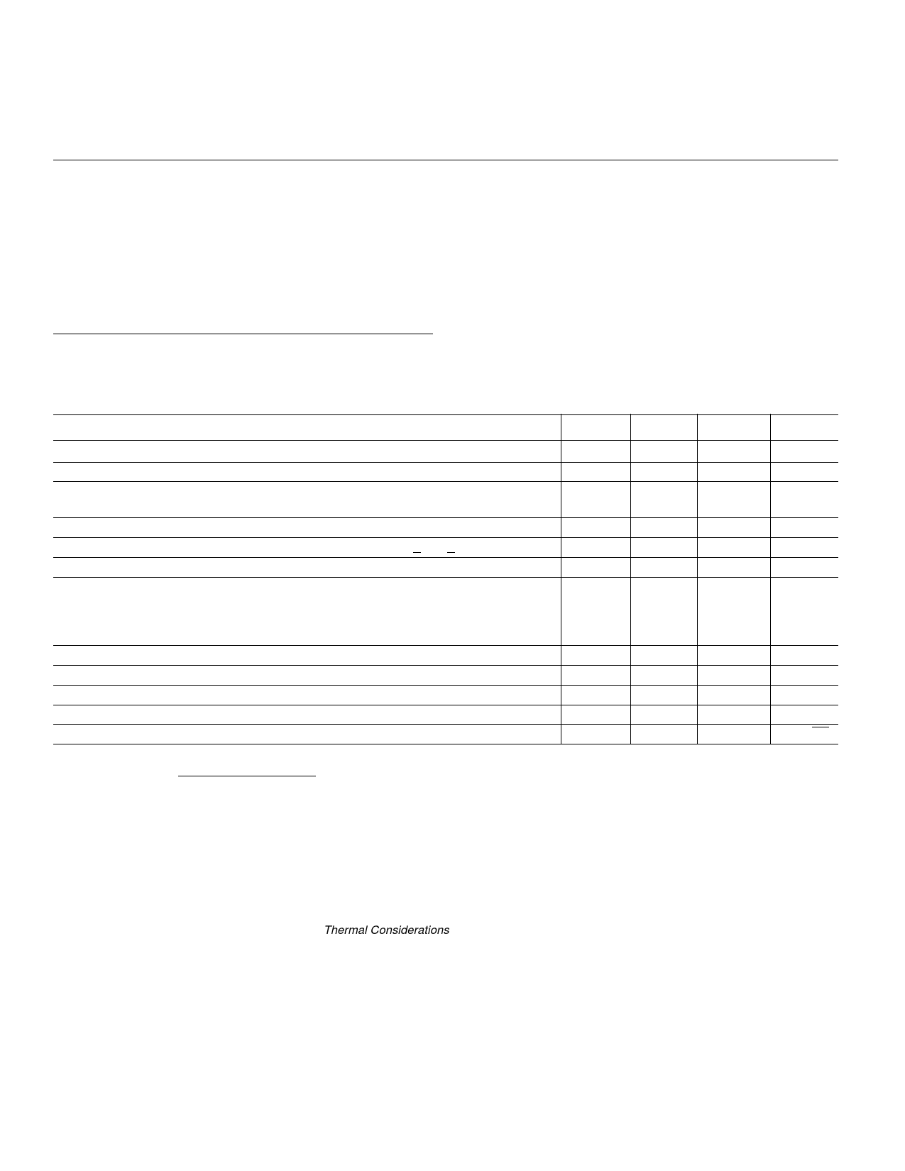
ELECTRICAL CHARACTERISTICS: VIN = VOUT + 1V, IL = 100µA, CL = 3.3µF, TA = 25°C, unless otherwise specified.
BOLDFACE type specifications apply for junction temperatures of – 40°C to +125°C.
Symbol
Parameter
Test Conditions
Min
Typ
Max
Units
VIN
Input Operating Voltage
—
—
6.0
V
IOUTMAX
VOUT
Maximum Output Current
Output Voltage
Note 1
300
—
—
mA
— VR ± 0.5%
—
V
VR – 2.5% —
VR + 2.5%
∆VOUT/∆T
VOUT Temperature Coefficient Note 2
—
40
—
ppm/°C
∆VOUT/∆VIN Line Regulation
(VR + 1V) < VIN < 6V
—
0.05
0.35
%
∆VOUT/VOUT
VIN – VOUT
Load Regulation
Dropout Voltage
IL = 0.1mA to IOUTMAX (Note 3)
IL = 0.1mA
IL = 100mA
IL = 300mA
(Note 4)
—
1.1
2.0
%
—
20
30
mV
—
80
160
—
270
480
IDD
Supply Current
—
50
90
µA
PSRR
Power Supply Rejection Ratio FRE ≤ 1kHz
—
60
—
dB
IOUTSC
Output Short Circuit Current
VOUT = 0V
—
550
650
mA
∆VOUT/∆PD Thermal Regulation
Note 5
—
0.04
—
V/W
eN
Output Noise
F = 10kHz, COUT = 1µF, RLOAD = 50Ω —
260
—
nV/√Hz
NOTES: 1. VR is the regulator output voltage setting.
2. TC VOUT = (VOUTMAX – VOUTMIN) x 10 6
VOUT x ∆T
3. Regulation is measured at a constant junction temperature using low duty cycle pulse testing. Load regulation is tested over a load
range from 0.1mA to the maximum specified output current. Changes in output voltage due to heating effects are covered by the thermal
regulation specification.
4. Dropout voltage is defined as the input to output differential at which the output voltage drops 2% below its nominal value measured at a
1V differential.
5. Thermal Regulation is defined as the change in output voltage at a time T after a change in power dissipation is applied, excluding load
or line regulation effects. Specifications are for a current pulse equal to ILMAX at VIN = 6V for T = 10msec.
6. The maximum allowable power dissipation is a function of ambient temperature, the maximum allowable junction temperature, and the
thermal resistance from junction-to-air (i.e. TA, TJ, θJA). Exceeding the maximum allowable power dissipation causes the device to
initiate thermal shutdown. Please see Thermal Considerations section of this data sheet for more details.
TC1108-2 1/25/00
2
Share Link: 