TC1015EV データシートの表示(PDF) - TelCom Semiconductor, Inc
部品番号
コンポーネント説明
メーカー
TC1015EV Datasheet PDF : 6 Pages
| |||
300mA CMOS LDO
TC1108
DETAILED DESCRIPTION
The TC1108 is a precision, fixed output LDO. Unlike
bipolar regulators, the TC1108 supply current does not
increase with load current. In addition, VOUT remains stable
and within regulation at very low load currents (an important
consideration in RTC and CMOS RAM battery backup
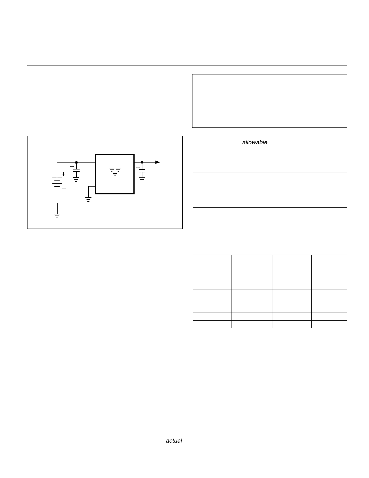
applications). Figure 1 shows a typical application circuit.
Battery
1 VIN
3
VOUT
VOUT
C1
C2
1µF
2
TC1108
1µF
GND
Figure 1: Typical Application Circuit
Output Capacitor
A 1µF (min) capacitor from VOUT to ground is required.
The output capacitor should have an effective series resis-
tance of 5Ω or less. A 1µF capacitor should be connected
from VIN to GND if there is more than 10 inches of wire
between the regulator and the AC filter capacitor, or if a
battery is used as the power source. Aluminum electrolytic
or tantalum capacitor types can be used. (Since many
aluminum electrolytic capacitors freeze at approximately –
30°C, solid tantalums are recommended for applications
operating below – 25°C.) When operating from sources
other than batteries, supply-noise rejection and transient
response can be improved by increasing the value of the
input and output capacitors and employing passive filtering
techniques.
Thermal Considerations
Thermal Shutdown
Integrated thermal protection circuitry shuts the regula-
tor off when die temperature exceeds 150°C. The regulator
remains off until the die temperature drops to approximately
140°C.
Power Dissipation
The amount of power the regulator dissipates is prima-
rily a function of input and output voltage, and output current.
The following equation is used to calculate worst case actual
power dissipation:
PD ≈ (VINMAX – VOUTMIN)ILOADMAX
Where:
PD = worst case actual power dissipation
VINMAX = maximum voltage on VIN
VOUTMIN = minimum regulator output voltage
ILOADMAX = maximum output (load) current
Equation 1.
The maximum allowable power dissipation (Equation 2)
is a function of the maximum ambient temperature (TAMAX),
the maximum allowable die temperature (TJMAX) and the
thermal resistance from junction-to-air (JA).
PDMAX =
(TJMAX – TAMAX)
JA
Where all terms are previously defined.
Equation 2.
Table 1 shows various values of JA for the TC1108
mounted on a 1/16 inch, 2-layer PCB with 1 oz. copper foil.
Table 1. Thermal Resistance Guidelines for TC1108
Copper
Area
(Topside)*
Copper
Area
(Backside)
Board
Area
Thermal
Resistance
(JA)
2500 sq mm
1000 sq mm
225 sq mm
100 sq mm
1000 sq mm
1000 sq mm
2500 sq mm
2500 sq mm
2500 sq mm
2500 sq mm
1000 sq mm
0 sq mm
2500 sq mm
2500 sq mm
2500 sq mm
2500 sq mm
1000 sq mm
1000 sq mm
45°C/W
45°C/W
53°C/W
59°C/W
52°C/W
55°C/W
NOTES: *Tab of device attached to topside copper
Equation 1 can be used in conjunction with Equation 2
to ensure regulator thermal operation is within limits. For
example:
GIVEN: VINMAX = 3.3V + 10%
VOUTMIN = 2.7V - 0.5%
ILOADMAX = 275mA
TJMAX = 125°C
TAMAX = 95°C
JA = 59°C/W
FIND: 1. Actual power dissipation
2. Maximum allowable dissipation
TC1108-2 1/25/00
3
Share Link: 