ICX209 データシートの表示(PDF) - Sony Semiconductor
部品番号
コンポーネント説明
メーカー
ICX209 Datasheet PDF : 18 Pages
| |||
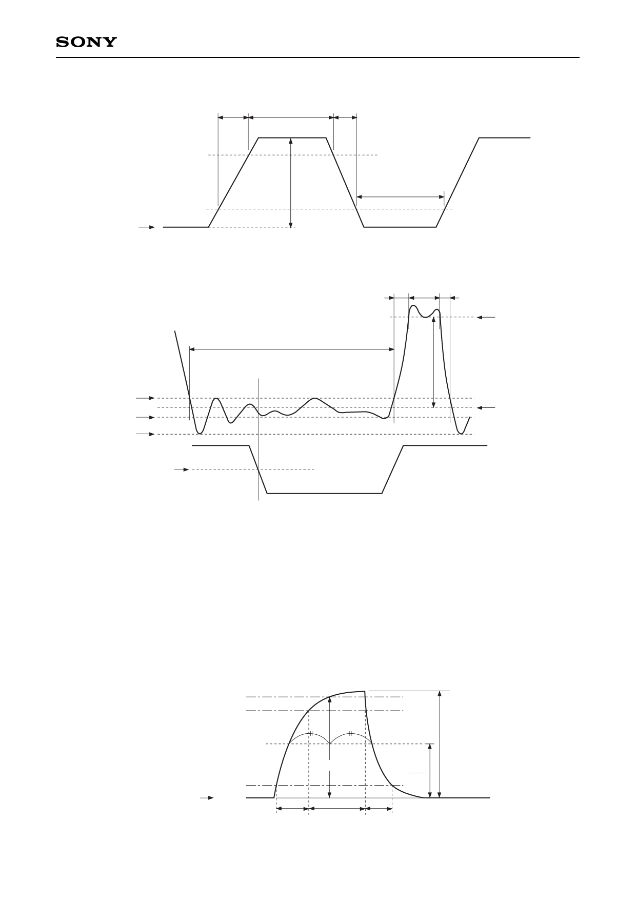
(3) Horizontal transfer clock waveform
tr
twh
tf
90%
10%
VHL
VφH
twl
(4) Reset gate clock waveform
tr
twh
tf
RG waveform
VRGLH
VRGLL
VRGLm
Hφ1 waveform
VφH/2 [V]
twl
Point A
VφRG
ICX209AK
VRGH
VRGL
VRGLH is the maximum value and VRGLL is the minimum value of the coupling waveform during the period from
Point A in the above diagram until the rising edge of RG. In addition, VRGL is the average value of VRGLH and
VRGLL.
VRGL = (VRGLH + VRGLL)/2
Assuming VRGH is the minimum value during the interval twh, then:
VφRG = VRGH – VRGL
Negative overshoot level during the falling edge of RG is VRGLm.
(5) Substrate clock waveform
100%
90%
10%
VSUB
0%
(A bias generated within the CCD)
VφSUB
tr
twh
φM
φM
2
tf
–6–
Share Link: 