SN74LS669 データシートの表示(PDF) - ON Semiconductor
部品番号
コンポーネント説明
メーカー
SN74LS669 Datasheet PDF : 4 Pages
| |||
SN74LS669
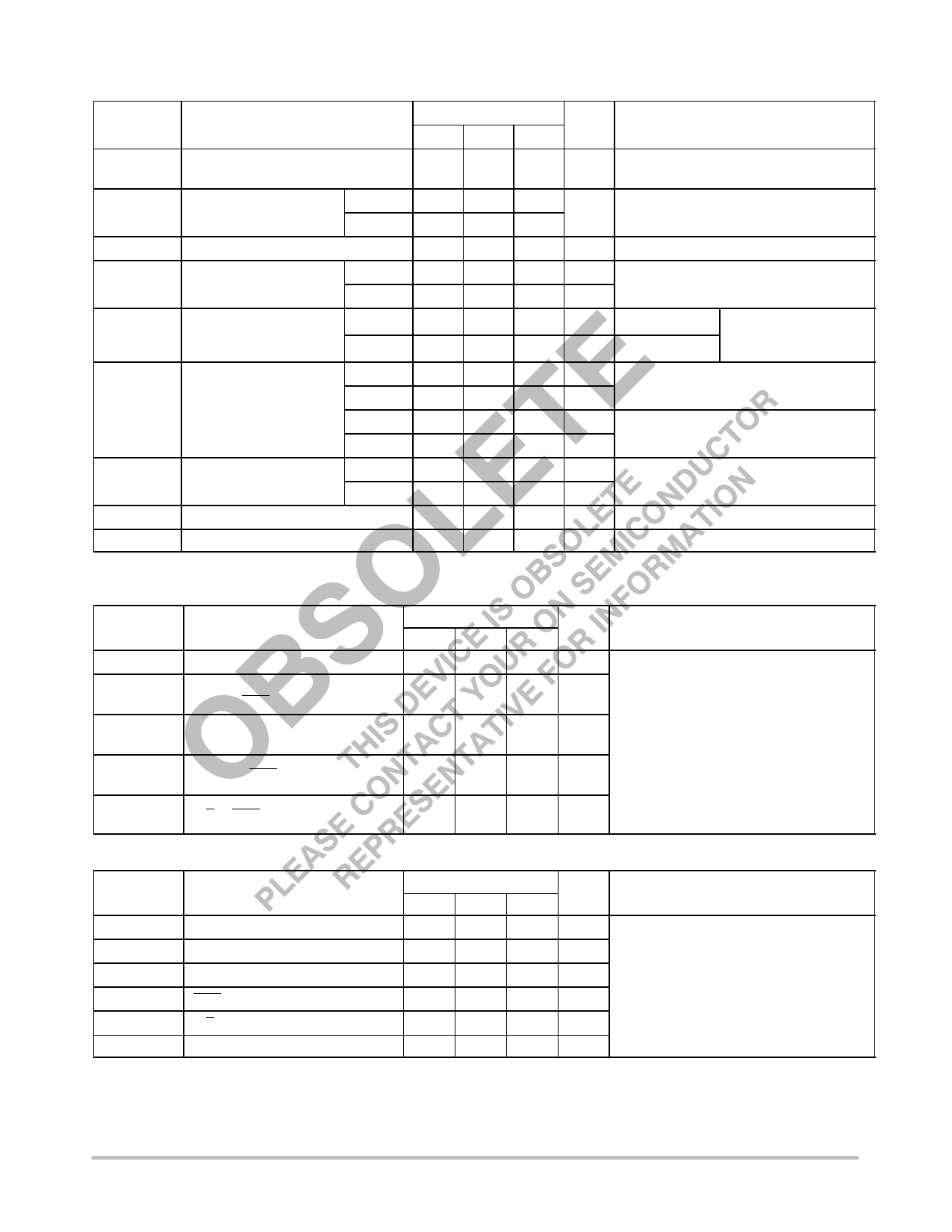
DC CHARACTERISTICS OVER OPERATING TEMPERATURE RANGE (unless otherwise specified)
Limits
Symbol
VIH
Parameter
Input HIGH Voltage
Min Typ Max Unit
Test Conditions
2.0
V
Guaranteed Input HIGH Voltage for
All Inputs
54
VIL
Input LOW Voltage
74
0.7
0.8
V
Guaranteed Input LOW Voltage for
All Inputs
VIK
Input Clamp Diode Voltage
−0.65 −1.5
V
VCC = MIN, IIN = − 18 mA
54
2.5
3.5
VOH
Output HIGH Voltage
74
2.7
3.5
V
VCC = MIN, IOH = MAX, VIN = VIH
V
or VIL per Truth Table
54, 74
VOL
Output LOW Voltage
74
Others
Enable T
IIH
Input HIGH Current
Others
Enable T
0.25 0.4
0.35 0.5
20
40
0.1
0.2
V
IOL = 4.0 mA
V
IOL = 8.0 mA
VCC = VCC MIN,
VIN = VIL or VIH
per Truth Table
μA
μA
VCC = MAX, VIN = 2.7 V
mA
VCC = MAX, VIN = 7.0 V
mA
Others
IIL
Input LOW Current
Enable T
−0.4 mA
−0.8
mA
VCC = MAX, VIN = 0.4 V
IOS
Short Circuit Current (Note 1)
− 20
−100 mA VCC = MAX
ICC
Power Supply Current
34
Note 1: Not more than one output should be shorted at a time, nor for more than 1 second.
mA VCC = MAX
AC CHARACTERISTICS (TA = 25°C, VCC = 5.0 V)
Symbol
fMAX
tPLH
tPHL
tPLH
tPHL
tPLH
tPHL
tPLH
tPHL
Parameter
Maximum Clock Frequency
Propagation Delay,
Clock to RCO
Propagation Delay,
Clock to Any Q
Enable to RCO
U/D to RCO
Limits
Min Typ Max
25
32
26
40
40
60
18
27
18
27
11
17
29
45
22
35
26
40
Unit
MHz
ns
ns
ns
ns
Test Conditions
CL = 15 pF
AC SETUP REQUIREMENTS (TA = 25°C)
Symbol
tW
ts
ts
ts
ts
th
Parameter
Clock Pulse Width
Data Setup Time
Enable Setup Time
Load Setup Time
U/D Setup Time
Hold Time, Any Input
Limits
Min Typ Max Unit
20
ns
20
ns
35
ns
25
ns
30
ns
0
ns
Test Conditions
VCC = 5.0 V
http://onsemi.com
3
Share Link: 