HV5222 データシートの表示(PDF) - Supertex Inc
部品番号
コンポーネント説明
メーカー
HV5222 Datasheet PDF : 10 Pages
| |||
HV5222
44-Lead PLCC Pin Assignment (PJ)
HV5222PJ
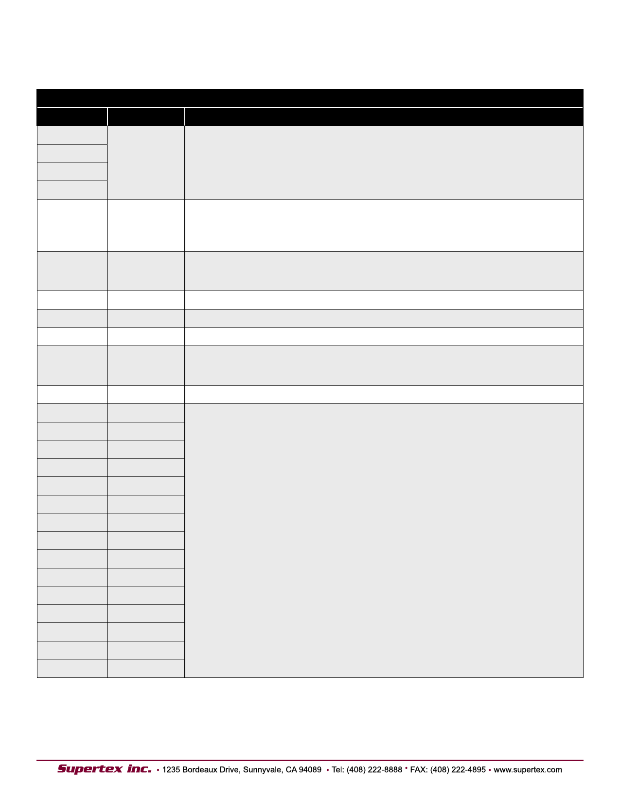
Pin
Function Description
19
20
N/C
No connect.
21
22
Output enable input.
23
OE
When OE is LOW, all HV outputs are forced into a LOW state, regardless of data in
each channel. When OE is HIGH, all HV outputs reflect data latched.
Data shift register clock.
24
CLK
Input are shifted into the shift register on the positive edge of the clock.
25
GND
Logic and high voltage ground.
26
VDD
Low voltage logic power rail.
27
STR
Strobe.
Serial data input
28
DATA IN
Data needs to be present before each rising edge of the clock.
29
N/C
No connect
30
HVOUT32
31
HVOUT31
32
HVOUT30
33
HVOUT29
34
HVOUT28
35
HVOUT27
36
HVOUT26
37
HVOUT25
High voltage outputs.
38
HVOUT24
39
HVOUT23
40
HVOUT22
41
HVOUT21
42
HVOUT20
43
HVOUT19
44
HVOUT18
7
Share Link: 